Active light sensitive or radiation sensitive resin composition, active light sensitive or radiation sensitive film, mask blank provided with active light sensitive or radiation sensitive film, pattern forming method, method for manufacturing electronic device, electronic device and novel compound

a technology of active light or radiation sensitive resin and film, which is applied in the direction of photosensitive materials, instruments, photomechanical equipment, etc., can solve the problems of difficult to find suitable, the current situation cannot be said to be sufficient, and the resolution of isolated line patterns is likely to deteriorate, etc., to achieve excellent pattern shape, low line edge roughness, and high resolving power

Active Publication Date: 2016-07-21
FUJIFILM CORP
View PDF7 Cites 2 Cited by
  • Summary
  • Abstract
  • Description
  • Claims
  • Application Information

AI Technical Summary

Benefits of technology

[0066]By the present invention, it is possible to provide an active light sensitive or radiation sensitive resin composition of which a pattern which satisfies high resolving power, an excellent pattern shape, and low line edge roughness (LER) can be formed, an active light sensitive or radiation sensitive film using this composition, a mask blank having this film, and a pattern forming method. According to the present invention, it is possible to suppress reduction in resolution even in a case where an ultra fine (for example, a line width of 50 nm or less) pattern is formed by exposure using an electron beam or extreme ultraviolet rays.

Problems solved by technology

However, from the viewpoint of total performance as a resist, it is extremely difficult to find a suitable combination of a resin, a photoacid generator, a basic compound, an additive, and a solvent, used, and, in particular, in view of recent demand for forming an ultra fine (for example, a line width of 50 nm or less) pattern with high performance, the current situation cannot yet be said to be sufficient.
Accordingly, for example, if the accelerating voltage of the EB is increased, resolution of the isolated line pattern is likely to deteriorate.
Consequently, in a case where the isolated line pattern is formed on the photomask blanks, there is a possibility that the pattern will be easily influenced particularly by the backward scattering and that the resolution will deteriorate.
On the other hand, in EUV (Extreme Ultra Violet) lithography, due to the surface topology of a reflecting mirror configuring the optical system of an exposure device or flare light generated by a phase difference, and unintended light (Out of Band light: OoB light) of a wavelength different from EUV light, which is generated since the reflecting mirror shows a certain degree of reflection characteristics for even light of a wavelength different from the exposure wavelength (typically, 13.5 nm) of the EUV light, decrease in resolution is likely to be caused.
However, due to the influence of swelling of a resist film at the time of development, elimination of the pattern collapse is not sufficient.
These cross-linking agents are discussed in JP1989-293339A (JP-H01-293339A), JP1994-301200A (JP-H06-301200A), and the like, and by using these cross-linking agents, the effect in which resolution is improved to some extent is obtained, but, in a resist film thinned for forming a fine pattern, it is not possible to obtain satisfactory results.
Accordingly, even in a case where an ultra fine (for example, a line width of 50 nm or less) pattern is formed by using X-rays, soft X-rays, or an electron beam as an exposure light source, it is important to satisfy high resolution and resist performance such as roughness characteristics at the same time, and thus, there is a problem that needs to be solved.

Method used


Image

  • Active light sensitive or radiation sensitive resin composition, active light sensitive or radiation sensitive film, mask blank provided with active light sensitive or radiation sensitive film, pattern forming method, method for manufacturing electronic device, electronic device and novel compound
  • Active light sensitive or radiation sensitive resin composition, active light sensitive or radiation sensitive film, mask blank provided with active light sensitive or radiation sensitive film, pattern forming method, method for manufacturing electronic device, electronic device and novel compound
  • Active light sensitive or radiation sensitive resin composition, active light sensitive or radiation sensitive film, mask blank provided with active light sensitive or radiation sensitive film, pattern forming method, method for manufacturing electronic device, electronic device and novel compound

Examples


examples

[0437]Hereinafter, the present invention will be described in further detail using examples, but the content of the invention is not limited thereto.

Synthesis of Cross-Linking Agent (C)

synthesis example

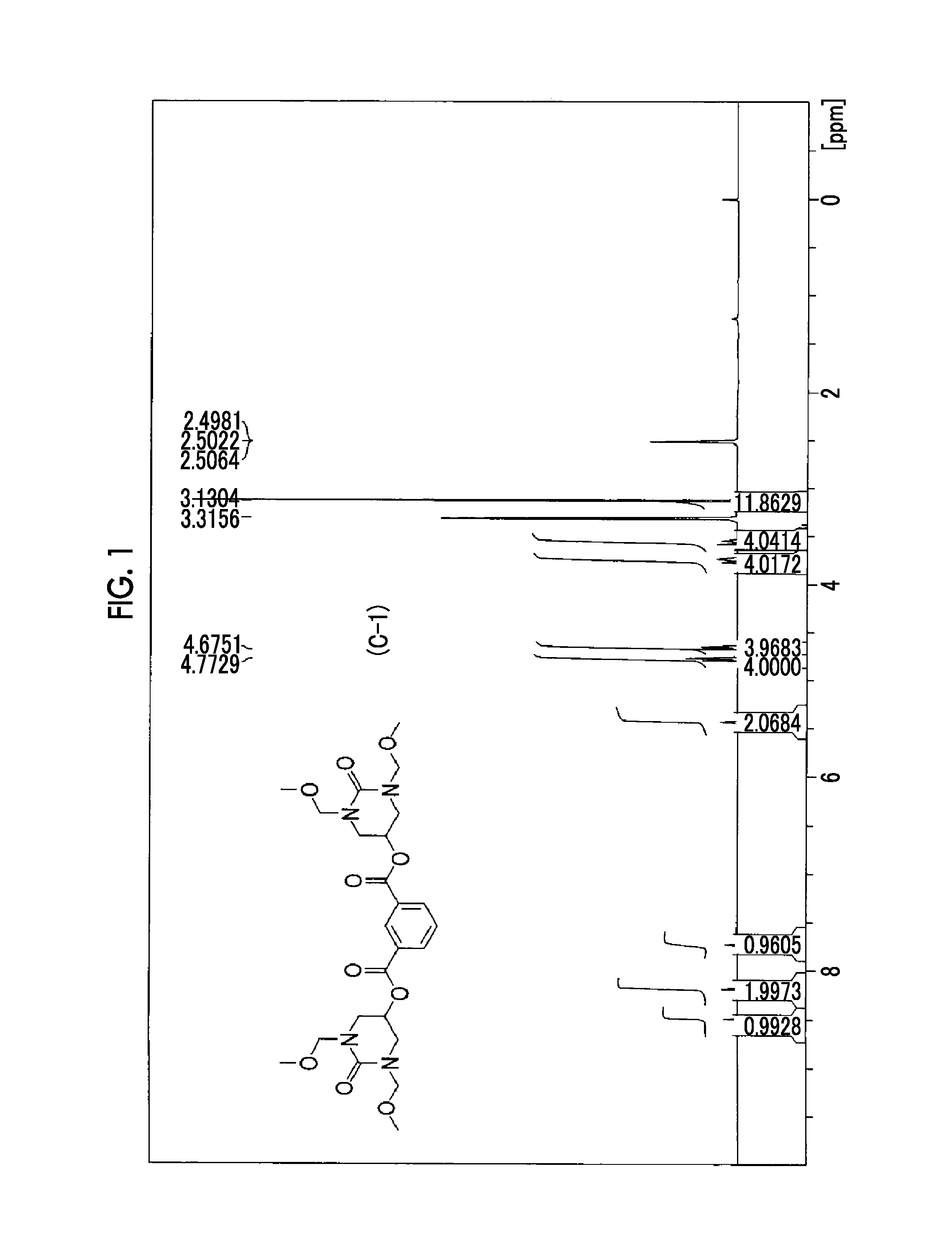
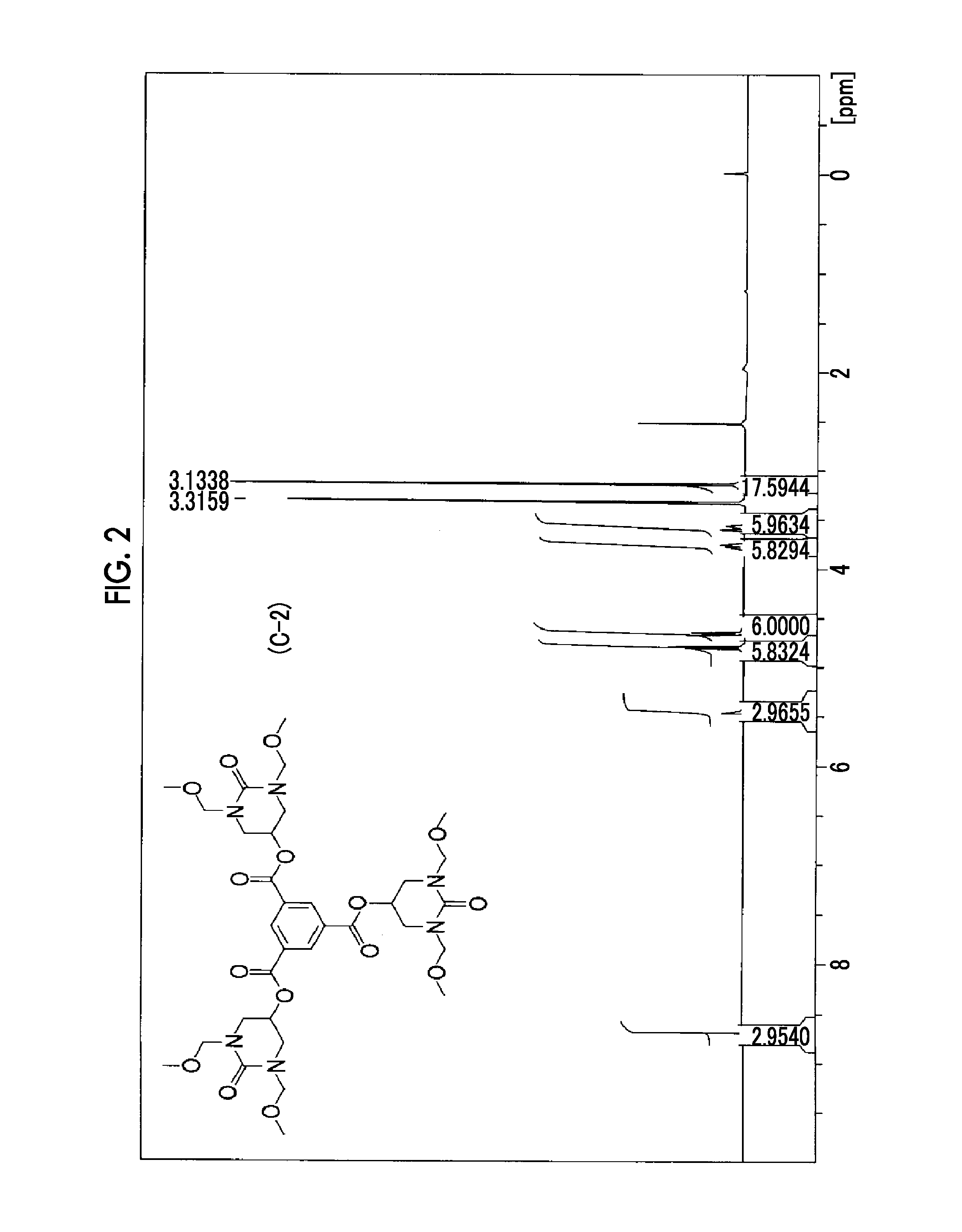
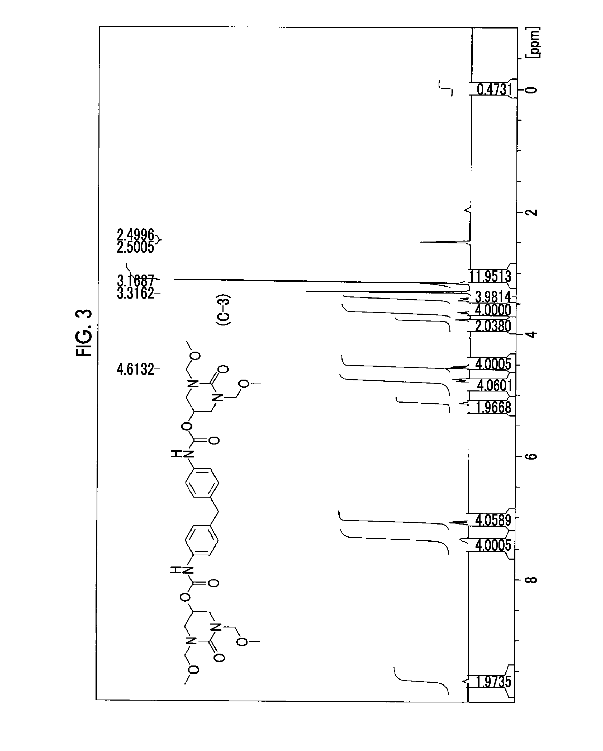
Synthesis of Compound C-1

[0438]

Synthesis of Compound 1

[0439]A compound 1 was synthesized by the method described in paragraphs “0119” and “0120” of JP2012-31233A.

Synthesis of Compound 3

[0440]The compound 1 (50 g) and paraformaldehyde (39 g) were mixed in DMAc (250 g) in a 2 L eggplant flask, and the pH of the reaction liquid was adjusted to 10 by adding a 1 N sodium hydroxide aqueous solution thereto. This mixture was stirred at room temperature for 3 hours, and production of a compound 2 was confirmed by NMR.

[0441]Methanol (500 g) was added to the reaction liquid including the obtained compound 2, and the pH of the reaction liquid was adjusted to 2 by adding concentrated sulfuric acid while ice-cooling. This reaction liquid was further stirred at room temperature for 1 hour, and production of a compound 3 was confirmed by NMR.

[0442]After 200 g of a saturated sodium bicarbonate water was added to this reaction liquid, the methanol was removed by distillation under reduced pressure, ...


PUM

PropertyMeasurementUnit
widthaaaaaaaaaa
thicknessaaaaaaaaaa
dispersityaaaaaaaaaa

Abstract

There is provided an active light sensitive or radiation sensitive resin composition which contains (A) an alkali soluble resin and (C) a cross-linking agent represented by the following General Formula (1-0).

Description

CROSS-REFERENCE TO RELATED APPLICATIONS[0001]This application is a Continuation application of PCT Application No. PCT / JP2014 / 075682, filed Sep. 26, 2014, and based upon and claiming the benefit of priority from Japanese Patent Application No. 2013-205970, filed Sep. 30, 2013, the entire contents of all of which are incorporated herein by reference.BACKGROUND OF THE INVENTION[0002]1. Field of the Invention[0003]The present invention relates to an active light sensitive or radiation sensitive resin composition that is suitably used for a production process of VLSIs and high-capacity microchips, a fabrication process of molds for nanoimprint, an ultramicrolithography process applicable for a production process of high-density information recording media, and other photofabrication processes, an active light sensitive or radiation sensitive film, a mask blank provided with the active light sensitive or radiation sensitive film, a pattern forming method, a method for manufacturing an el...

Claims


Application Information

Patent Timeline
Patent Type & Authority Applications(United States)
IPC IPC(8): G03F7/038G03F7/20C07D487/04C07C275/24C07C233/36G03F7/32C07D239/10
CPCG03F7/038G03F7/32G03F7/20C07D487/04C07C275/24C07C233/36C07D239/10C07C271/16C07C271/24C07C271/34C07C275/10C07C275/26C07C323/60C07C2601/14C07D211/26C07D233/32C07D233/36C07D235/26C07D251/30C07D403/12G03F7/0382C07D209/82C07D307/91C07D333/76G03F1/22G03F7/004G03F7/203G03F1/20G03F7/0387
Inventor YAMAGUCHI, SHUHEITSUCHIMURA, TOMOTAKAYOKOKAWA, NATSUMITAKAHASHI, KOUTAROU
Owner FUJIFILM CORP
Why Eureka
Try Eureka