Wafer holder and wafer conveyor system equipped with the same

a conveyor system and wafer technology, applied in the direction of conveyors, grinding drives, manufacturing tools, etc., can solve the problems of time loss in production, particle contamination, circuit devices formed on the wafers may become defective, etc., to reduce the contact area with the wafers and ensure the support of the wafers

Inactive Publication Date: 2005-10-06
SAMSUNG ELECTRONICS CO LTD
View PDF6 Cites 6 Cited by
  • Summary
  • Abstract
  • Description
  • Claims
  • Application Information

AI Technical Summary

Benefits of technology

[0011] In one aspect, the present invention provides a wafer holder to

Problems solved by technology

If a part is worn out, time is lost in production when the worn out part is maintained or replaced.
Furthermore, frictional wear in a system operating within a clean room environment may further cause parti

Method used


Image

  • Wafer holder and wafer conveyor system equipped with the same
  • Wafer holder and wafer conveyor system equipped with the same
  • Wafer holder and wafer conveyor system equipped with the same

Examples


Embodiment Construction

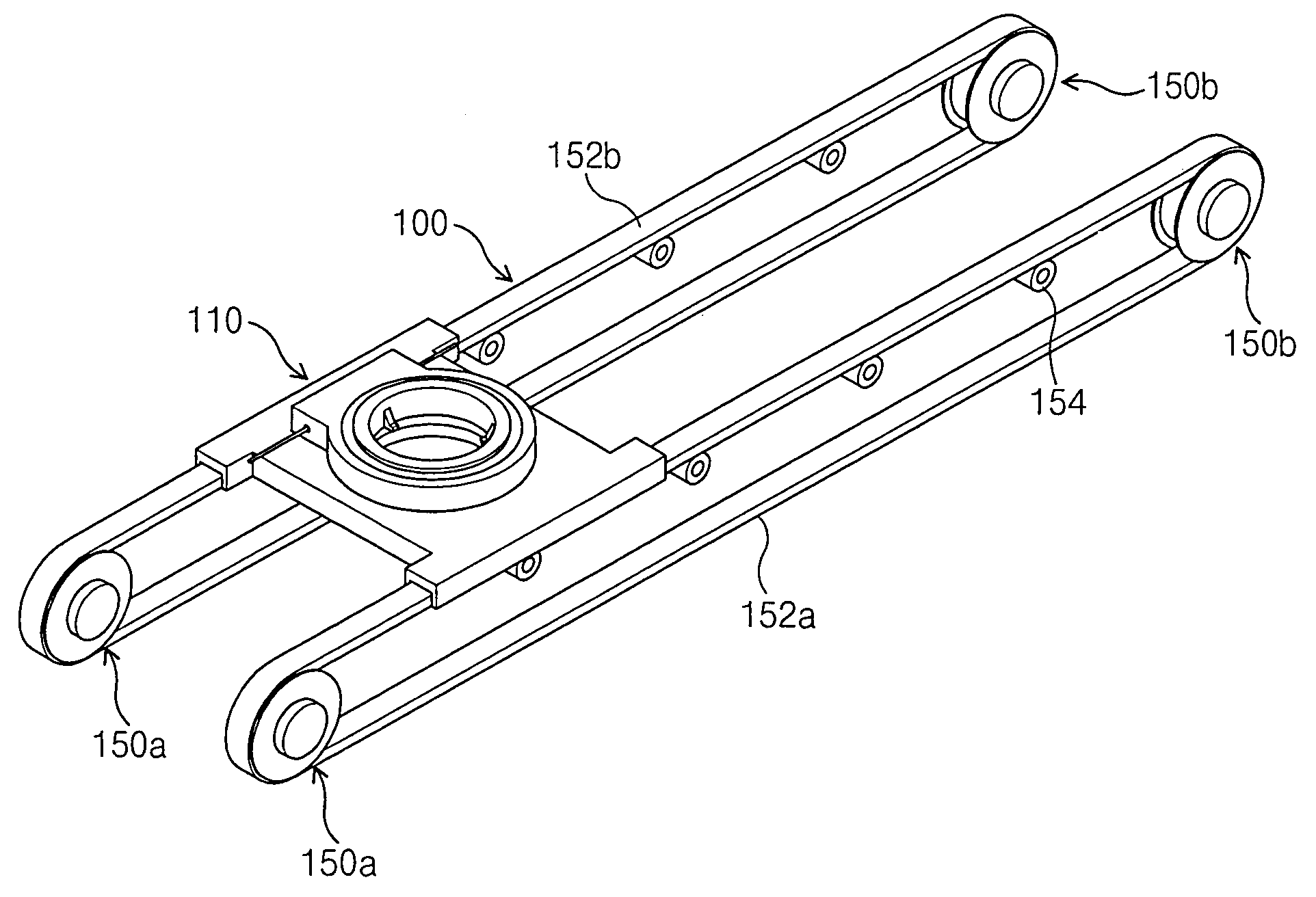
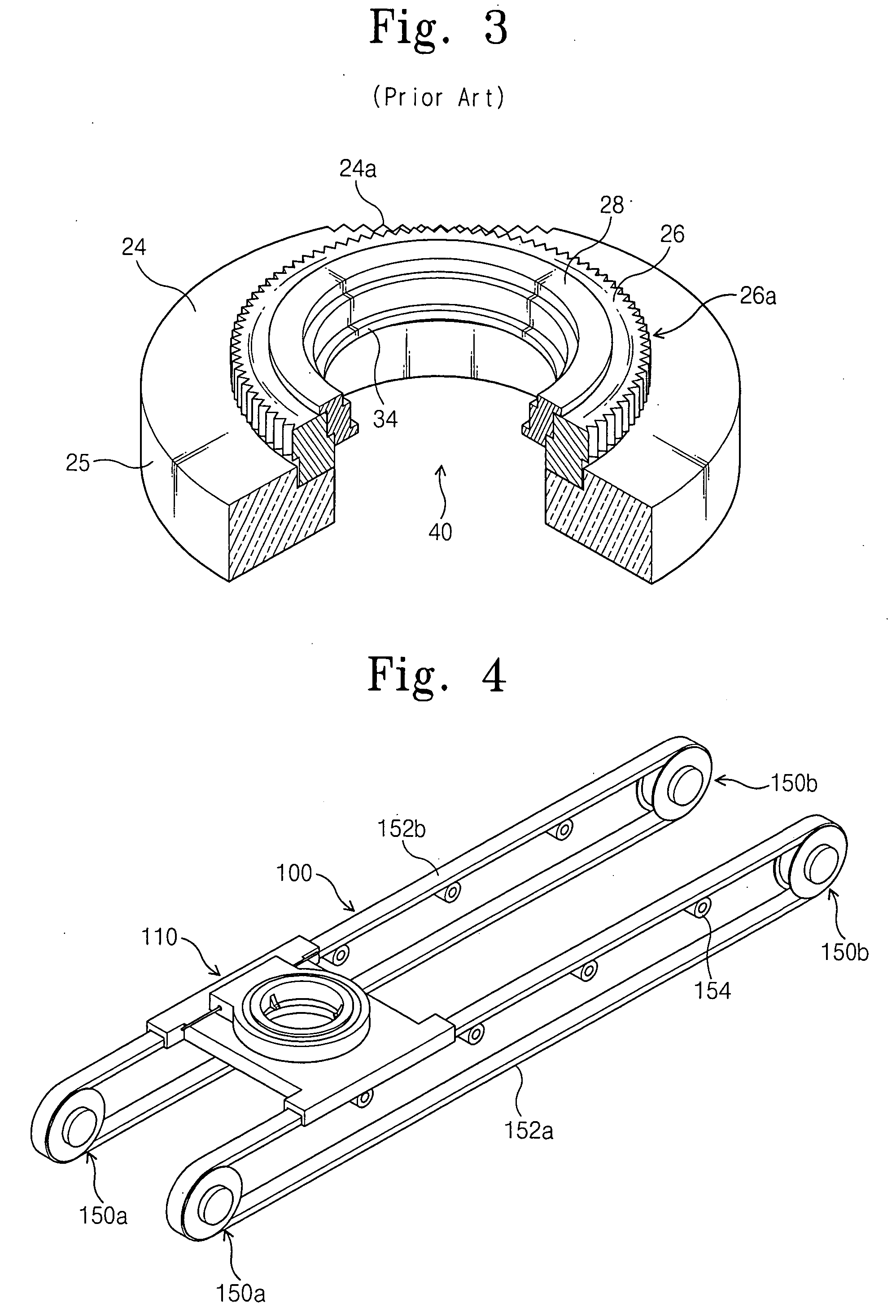
[0026] A wafer conveyor system 100 according to the present invention is illustrated in FIG. 4. Referring to FIG. 4, wafer conveyor system 100 comprises guide rails 152, further comprises a first guide rail 152a and a second guide 152b. A set of driving rollers 150a and a set of passive rollers 150b are spaced apart from each other, with each set having one roller disposed in relation to the first guide rail 152a and second guide rail 152b, respectively. The inner portion of guide rails 152a, 152b contacts and wraps around driving roller 150a and passive roller 150b.

[0027] A wafer holder 110 is disposed between first and second guide rails 152a, 152b, and horizontally moves within a chamber in response to the movement of guide rails 152a, 152b. Namely, wafer holder 110 is transferred between a preparation area and an operation area on conveyor system 100.

[0028] Wafer conveyor system 100 optionally comprises a plurality of sub-rollers 154 installed between respective combinations o...


PUM


Abstract

The present invention is directed to a wafer holder and a related wafer conveyor system. The wafer holder holds a wafer and moves horizontally within a chamber. A contact area between the wafer and the wafer holder is reduced, and potential contaminants generated by ear between components of the wafer holder are trapped by an airtight cover. Since the wafer holder moves horizontally while being fixed to a guide rail, the wafer conveyor system reduces friction between the guide rail and the wafer holder.

Description

BACKGROUND OF THE INVENTION [0001] 1. Field of the Invention [0002] The present invention generally relates to an apparatus for use in a semiconductor fabricating process. More specifically, the present invention relates to a wafer holder and a wafer conveyor system equipped with the wafer holder. [0003] A claim of priority is made to Korean Patent Application No. 2003-95618 filed on Dec. 23, 2003, the disclosure of which is incorporated herein by reference in its entirety. [0004] 2. Description of Related Art [0005] In a conventional semiconductor fabricating process, an integrated circuit device is fabricated by forming a pattern on a semiconductor wafer, and monitoring the pattern-formed wafer. From a preparation area, a wafer is transferred to an operating area for fabrication and testing. The wafer is placed on an apparatus with its pattern-formed front side or back side facing up depending on the configuration of the fabricating apparatus or the test apparatus. When the wafer'...

Claims


Application Information

Patent Timeline
IPC IPC(8): B24B5/00H01L21/68H01L21/677H01L21/683H01L21/687
CPCH01L21/6776H01L21/68785H01L21/68
Inventor KIM, TAE-KYOUNGJEE, YUN-JUNGSHIN, KYOUNG-SUJUN, CHUNG-SAM
Owner SAMSUNG ELECTRONICS CO LTD
Why Eureka
Try Eureka