

Display device and method for manufacturing the same
a technology for display devices and manufacturing methods, applied in the field of display devices, can solve the problems of suppressing display defects, generating display defects, and affecting the display effect, so as to prevent the exfoliation of transparent conductive thin films and the defect of the layer beneath them, suppress display defects
- Summary
- Abstract
- Description
- Claims
- Application Information
AI Technical Summary
Benefits of technology
Problems solved by technology
Method used
Image

Examples
embodiment 1
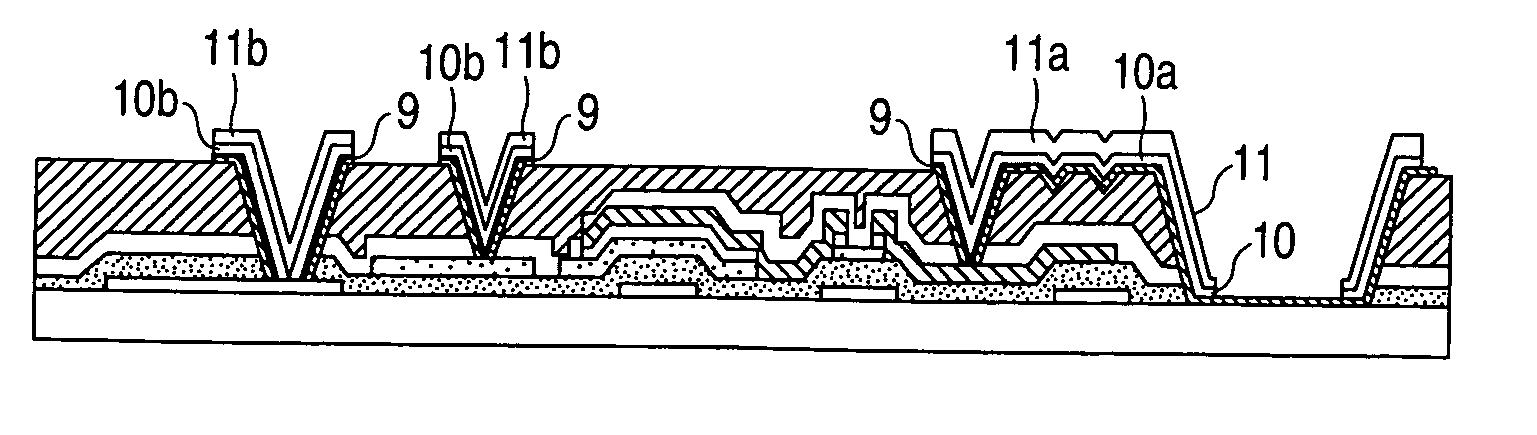
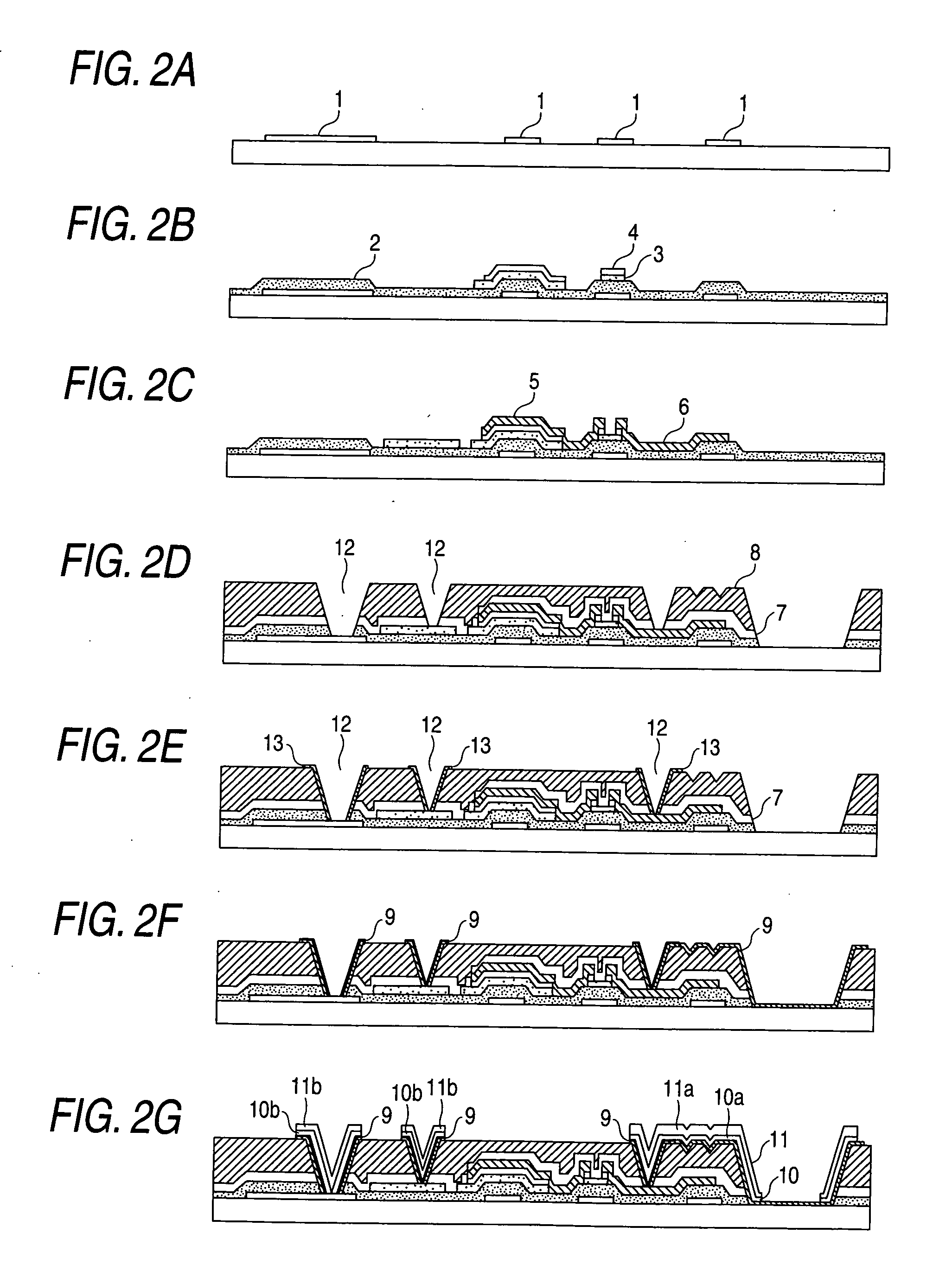
[0042] An explanation will be given of an embodiment in which this invention is applied to a semi-transmissive liquid crystal display device.
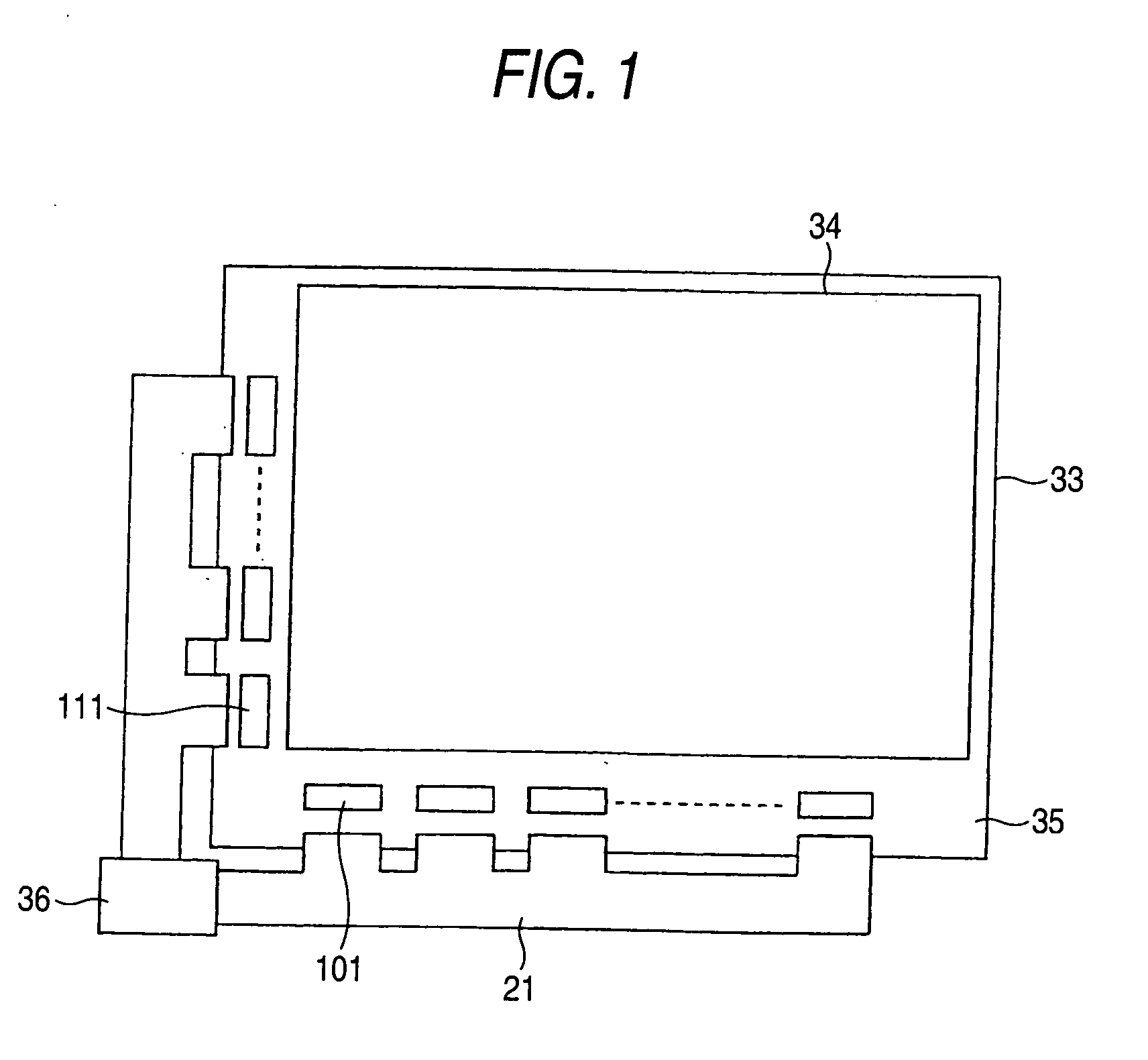
[0043]FIG. 1 is a top view showing the configuration of a liquid crystal display panel of a COG (Chip On Glass) liquid crystal display device. As seen from FIG. 1, a liquid crystal display panel 33 includes a display region 34 composed of a plurality of pixels arranged in a matrix shape and a frame region 35 formed on the outer periphery thereof. The liquid crystal display panel 33 also includes an array substrate in which an array circuit is formed and an opposite substrate thereto. Liquid crystal is sandwiched between these two substrates. Each of the pixels on the array substrate is equipped with a TFT which is a switching element for controlling input / output of a display signal.
[0044] Within the display region 34 on the array substrate, a plurality of source wirings and gate wirings are arranged in a matrix shape. The source wirings and g...
PUM
| Property | Measurement | Unit |
|---|---|---|
| thickness | aaaaa | aaaaa |
| thickness | aaaaa | aaaaa |
| thickness | aaaaa | aaaaa |
Abstract
Description
Claims
Application Information