Liquid crystal display device and electronic apparatus
a display device and liquid crystal technology, applied in non-linear optics, instruments, optics, etc., can solve the problems of reducing the degree of freedom of optical design, spotted pattern generation, narrow viewing angle of transmissive display, etc., to achieve wide viewing angle, suppress display defects, and good display characteristics
- Summary
- Abstract
- Description
- Claims
- Application Information
AI Technical Summary
Benefits of technology
Problems solved by technology
Method used
Image
Examples
third embodiment
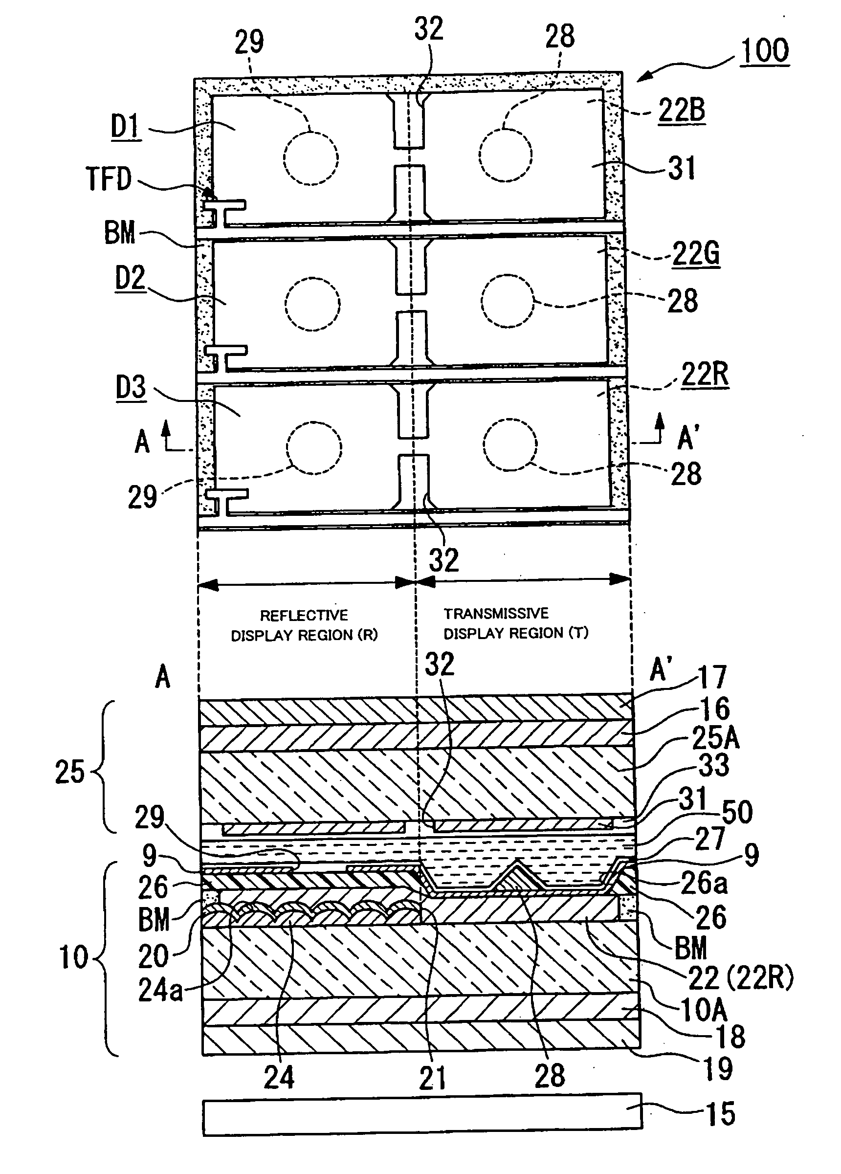
[0074] As shown in FIG. 6, in the liquid crystal display device 300 the convex portion 26a formed in the transmissive display region T and the insulating film 26 as a liquid-crystal-layer thickness-adjusting layer are formed in the same process, so that the convex portion 26a formed in the transmissive display region T is formed on the same layer with the same material as the insulating film 26.
[0075] In other words, resin layers having predetermined patterns are formed on the reflective display region R and the transmissive display region T. The resin layer on the reflective display region R is used as the insulating film 26 which is a liquid crystal thickness adjusting layer, and the resin layer on the transmissive display region T is used as the convex portion 26a for providing a convex shape to a sandwiching surface of the liquid crystal layer 50 in the transmissive display region T. In addition, a slit may be simultaneously formed in the electrode on the convex portion 26a in ...
first embodiment
[0082] Similarly, other examples of the liquid crystal display device 100 are constructed with the following conditions. The thickness of the liquid crystal layer in the transmissive display region T is 4.0 μm, the thickness of the liquid crystal layer in the reflective display region R is 2.0 μm, and the height of the convex portion 28 is 1.5 μm. On the inner surface of the lower substrate 10, the slit 29 or convex portion (instead of the slit) is formed in the reflective display region R. Various widths of the convex portion or the slit are selected. Then, contrasts in the reflective display of the examples evaluated are compared. The result of the comparison is shown in Table 2 as follows.
TABLE 2Width of convex portion or slit5 μm8 μm12 μmWhen the convex portion is formed in the9.68.76.8transmissive display regionWhen the slit is formed in the transmissive16.715.614.3display region
[0083] As shown in the table, it can be understood that, the spotted pattern are not detected in al...
PUM
| Property | Measurement | Unit |
|---|---|---|
| angle of inclination | aaaaa | aaaaa |
| angle | aaaaa | aaaaa |
| angle | aaaaa | aaaaa |
Abstract
Description
Claims
Application Information


