Electron-emitting device, electron source, and method for manufacturing image displaying apparatus
a technology of electron source and electron emission device, which is applied in the manufacture of electric discharge tube/lamp, discharge tube luminescnet screen, discharge tube/light tube, etc., can solve the problems of large wiring area on the substrate, large power consumption of the whole device, etc., and achieve good electron emission characteristics
- Summary
- Abstract
- Description
- Claims
- Application Information
AI Technical Summary
Benefits of technology
Problems solved by technology
Method used
Image
Examples
example 1
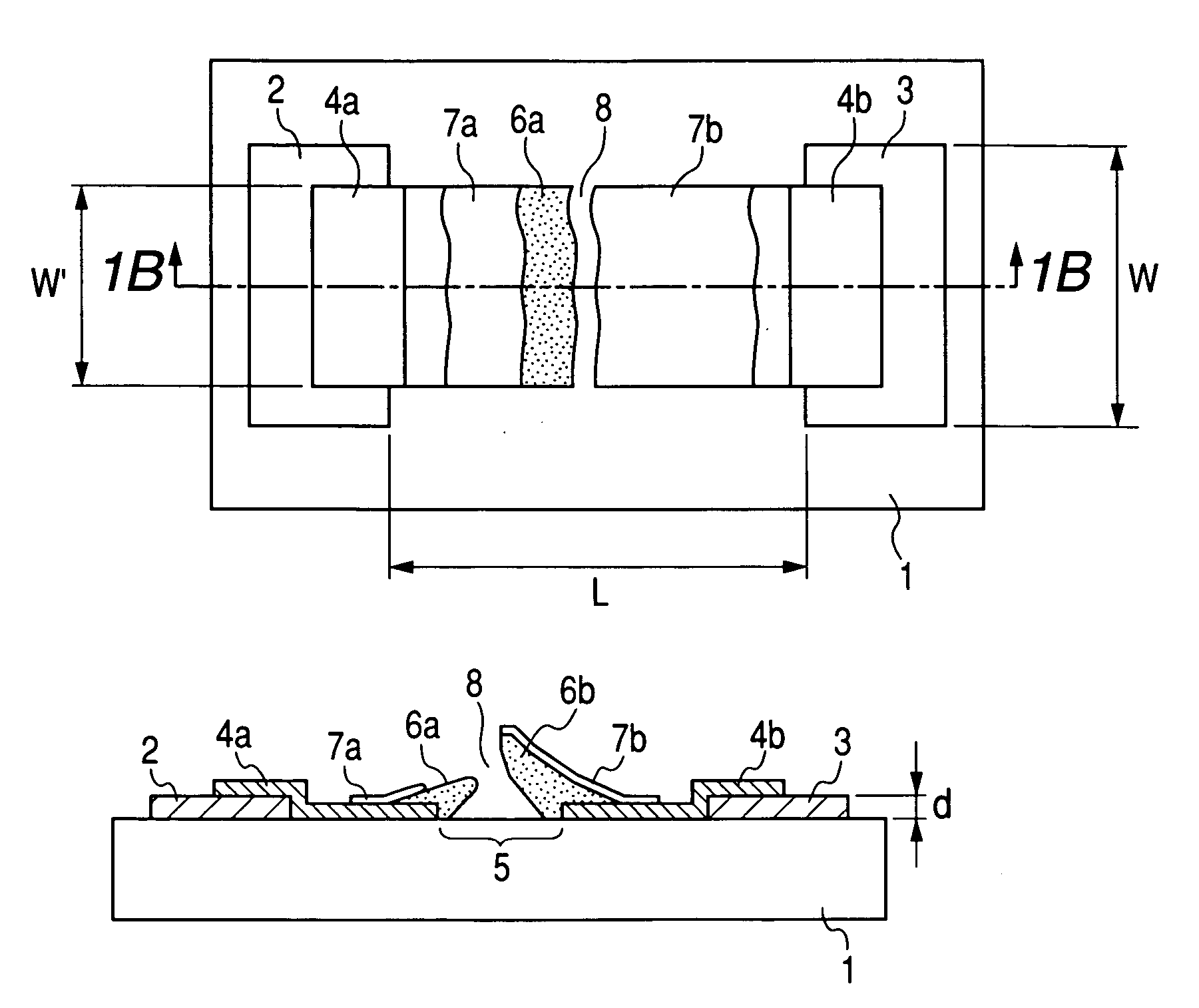
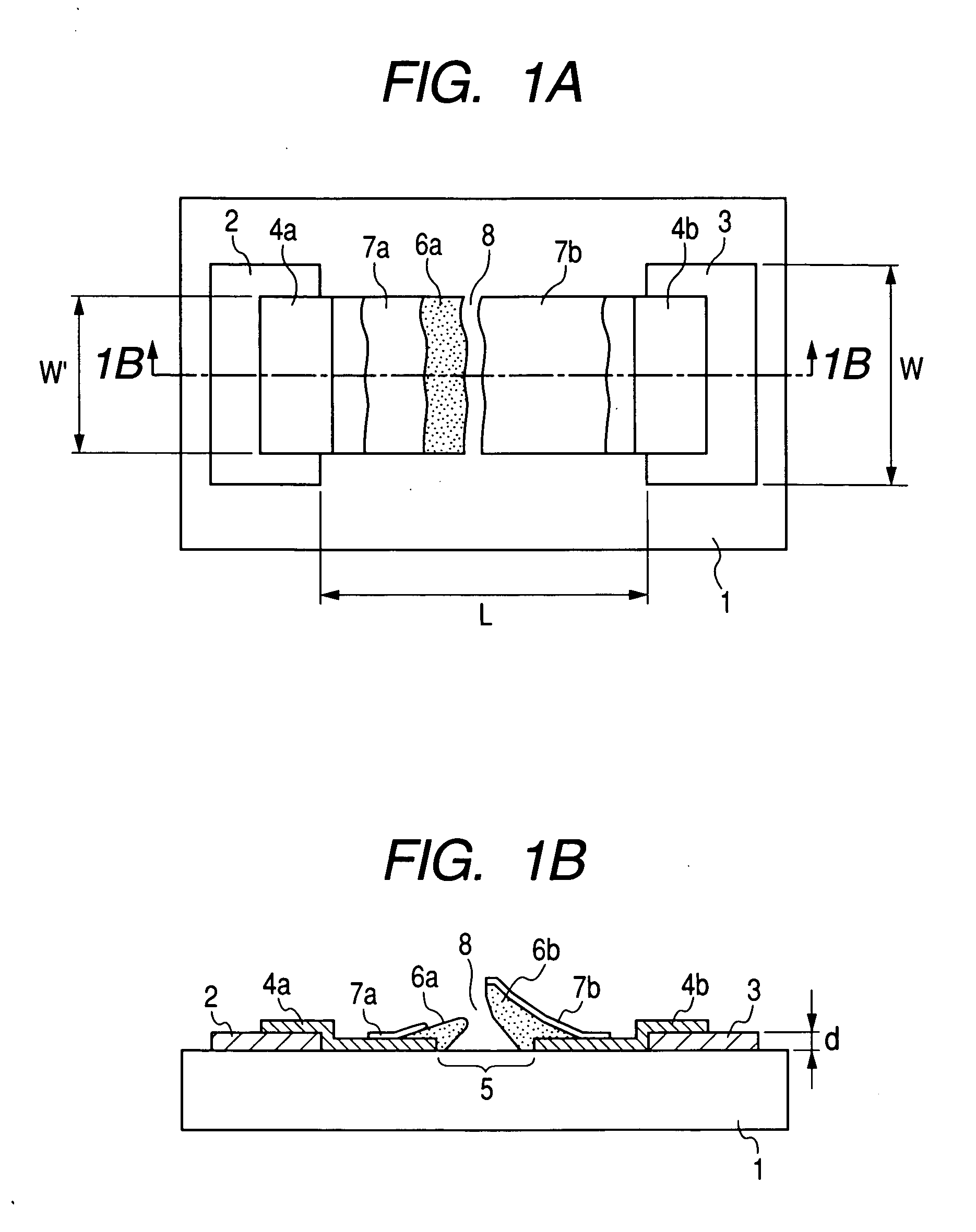
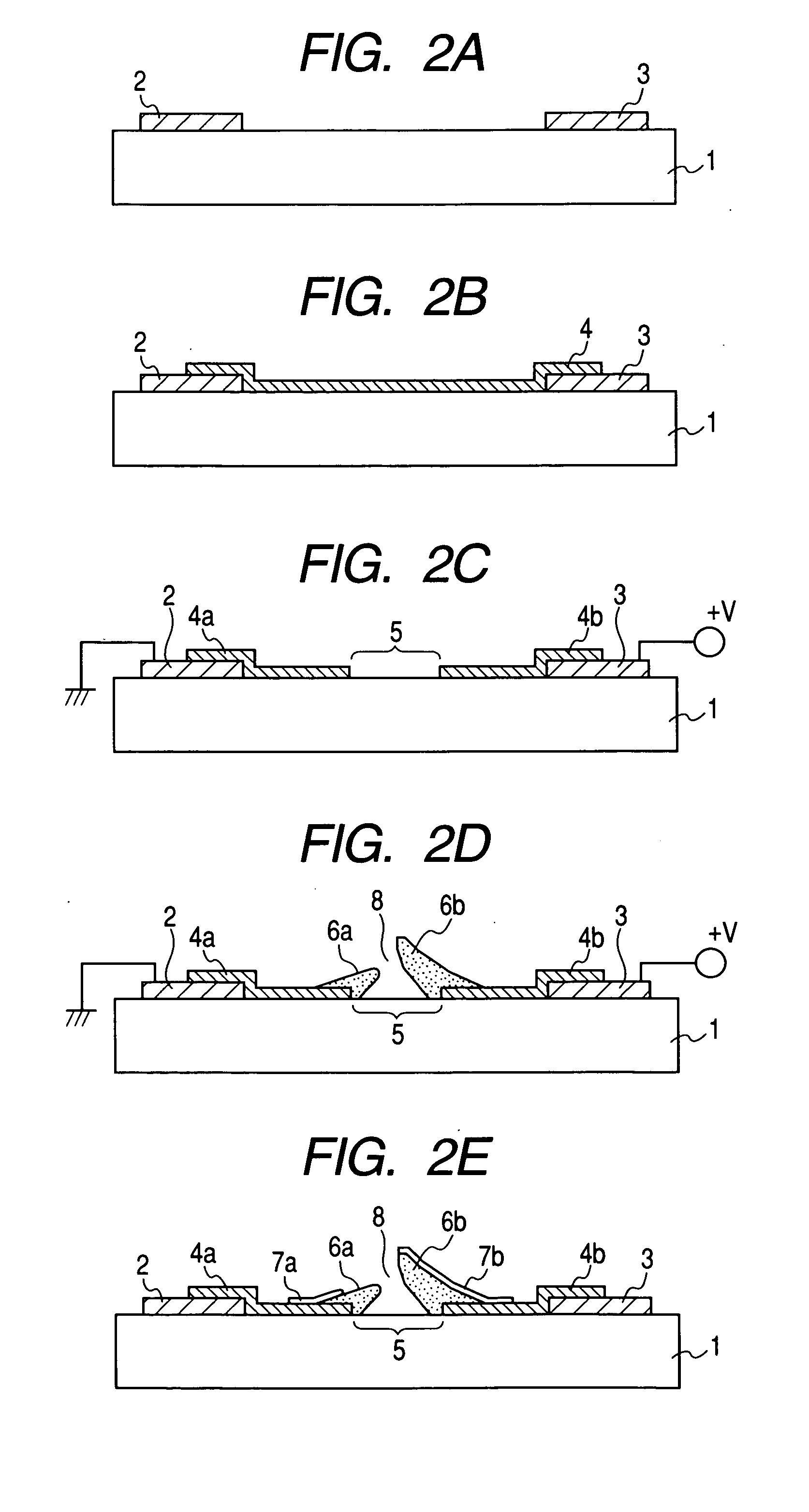
[0112] An electron-emitting device having the configuration shown in FIGS. 1A and 1B was produced in accordance with the processes shown in FIGS. 2A to 2E.
Process a
[0113] First, a pattern to be the device electrodes 2 and 3 and a desired gap L between the device electrodes 2 and 3 was formed on a cleaned quartz substrate 1 with photoresist (RD-2000N-41 made by Hitachi Chemical Co., Ltd.), and Ti and Pt were deposited to be the thicknesses of 5 nm and 30 nm, respectively, in order by the electron beam evaporation method. The photoresist pattern was dissolved by an organic solvent, and the lift off of the Pt / Ti deposition films were carried out. Then, the device electrode interval L was set to 3 μm, and the device electrodes 2 and 3 having the width W of 500 μm of the device electrodes were formed (FIG. 2A).
Process b
[0114] A Cr film having a film thickness of 100 nm was deposited by the vacuum evaporation, and the patterning was performed to have an opening corresponding to the ...
example 2
[0131] The processes of the Example 1 were performed until the Process d except that a substrate of soda lime glass with SiO2 coated thereon was used as the substrate 1.
Process e
[0132] In order to perform the activation process, tolunitrile was introduced in the vacuum apparatus through the slow leak valve, and the pressure of 1.0×10⁻⁴ Pa was maintained. Next, the activation processing of the device which had received the forming processing was performed with the waveform shown in FIG. 4, in which the pulse width T1 was set to 1 msec, the pulse width T1′ was set to 0.1 msec, the pulse interval T2 was set to 10 msec, and the maximum voltage values were set to ±22 V, through the device electrodes 2 and 3 of the device. In this case, the voltage given to the device electrode 3 was made to be positive, and the direction of the device current If flowing from the device electrode 3 to the device electrode 2 was positive. After confirming that the device current If had been saturated af...
example 3
[0144] An image displaying apparatus using an electron source in which electron-emitting devices were arranged in a passive matrix arrangement was produced. The manufacturing process thereof is described with reference to FIGS. 9 to 16.
[0145] A plurality of pairs of device electrodes 2 and 3 was formed on the substrate 1 (FIG. 9).
[0146] A substrate made by coating a SiO2 film to be a thickness of 100 nm as a sodium blocking layer on a sheet of glass having a thickness of 2.8 mm of PD-200 (made by Asahi Glass Co., Ltd.), which has little alkaline components, and by baking the sodium blocking layer was used as the substrate 1.
[0147] Further, a film of titanium Ti was formed to be a thickness of 5 nm on the glass substrate 1 and a film of platinum Pt was formed to be a thickness of 40 nm on the Ti film, both formed by the sputtering method as under coating layers. After that, photoresist was coated on the Pt film, and the patterning for forming the device electrodes 2 and 3 was perf...
PUM
 Abstract
Description
Claims
Application Information


