Electron-emitting device, electron source, and method for manufacturing image displaying apparatus

a technology of electron source and electron emission device, which is applied in the manufacture of electrode systems, discharge tubes, luminescent screens, etc., can solve the problems of large wiring area on the substrate, large power consumption of the whole device, etc., and achieve good electron emission characteristics

Inactive Publication Date: 2007-12-25
CANON KK
View PDF41 Cites 17 Cited by
  • Summary
  • Abstract
  • Description
  • Claims
  • Application Information

AI Technical Summary

Benefits of technology

[0009]It is an object of the present invention to provide an electron-emitting device realizing a good electron emission characteristic and the elongation of its life simultaneously, and a method for manufacturing the same. Moreover, it is another object of the present invention to provide an electron source and an image displaying apparatus, both using a plurality of the electron-emitting devices, and a method for manufacturing them.

Problems solved by technology

For this reason, not only the power consumption of the whole device becomes large, but also the ratio of the area which wiring occupies on a substrate becomes large, which serves as restrictions on the designing of an apparatus.

Method used


Image

  • Electron-emitting device, electron source, and method for manufacturing image displaying apparatus
  • Electron-emitting device, electron source, and method for manufacturing image displaying apparatus
  • Electron-emitting device, electron source, and method for manufacturing image displaying apparatus

Examples


example 1

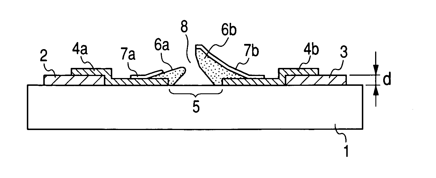
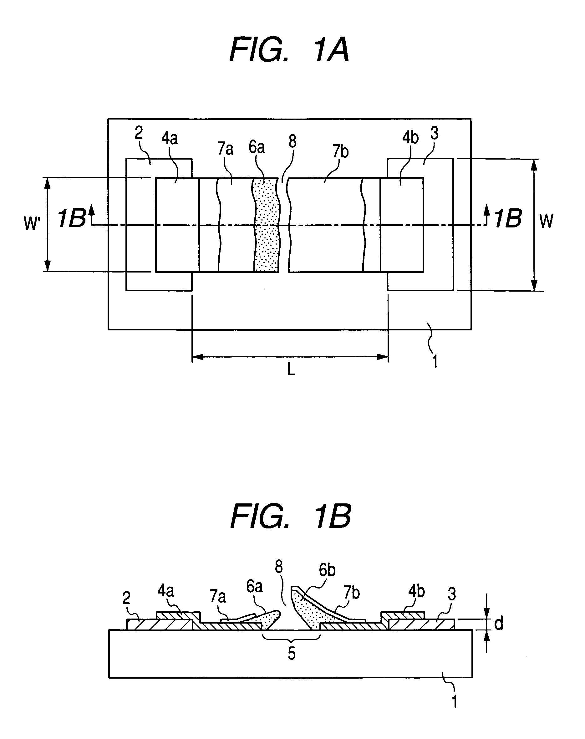
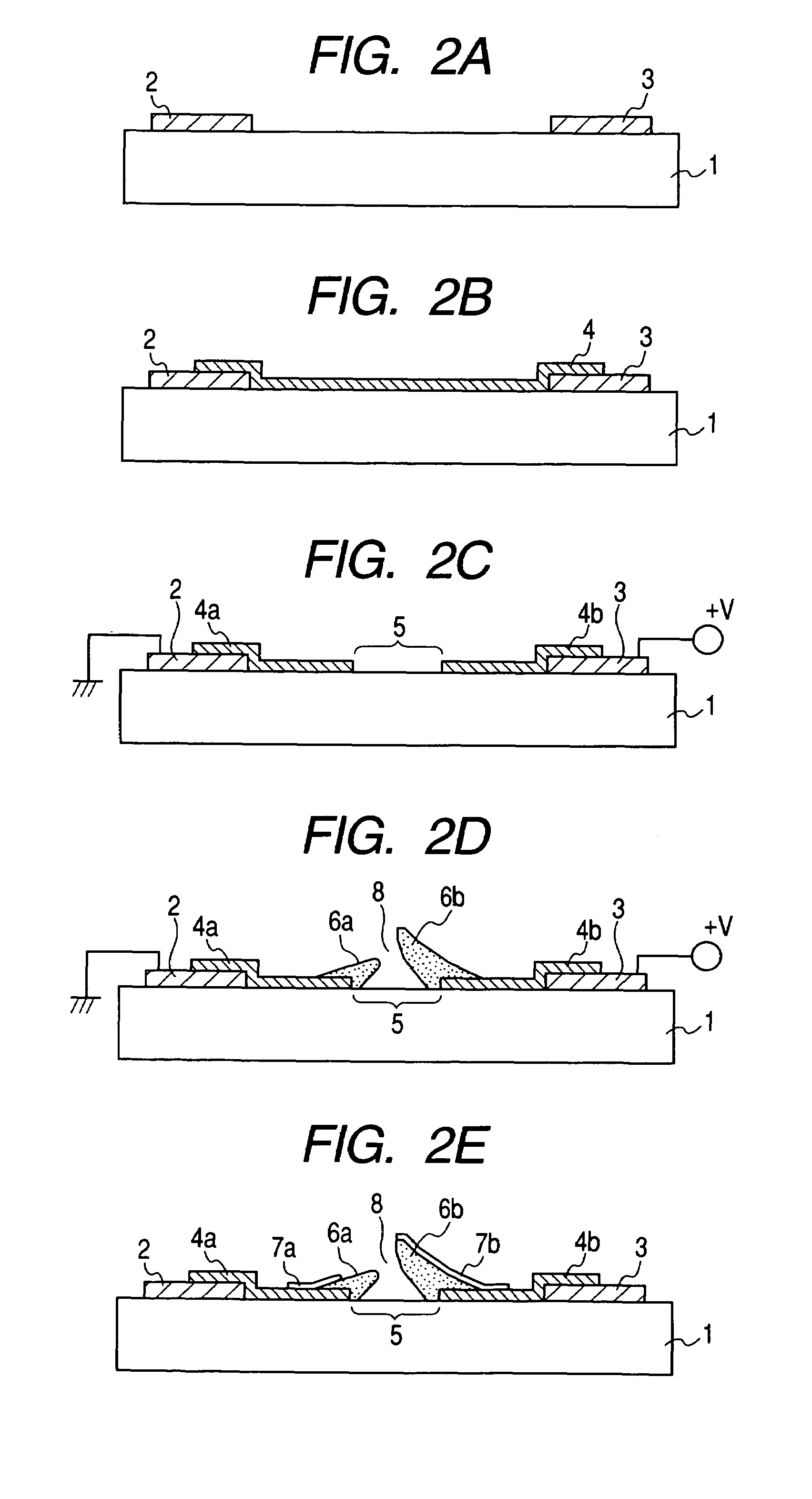
[0112]An electron-emitting device having the configuration shown in FIGS. 1A and 1B was produced in accordance with the processes shown in FIGS. 2A to 2E.

Process a

[0113]First, a pattern to be the device electrodes 2 and 3 and a desired gap L between the device electrodes 2 and 3 was formed on a cleaned quartz substrate 1 with photoresist (RD-2000N-41 made by Hitachi Chemical Co., Ltd.), and Ti and Pt were deposited to be the thicknesses of 5 nm and 30 nm, respectively, in order by the electron beam evaporation method. The photoresist pattern was dissolved by an organic solvent, and the lift off of the Pt / Ti deposition films were carried out. Then, the device electrode interval L was set to 3 μm, and the device electrodes 2 and 3 having the width W of 500 μm of the device electrodes were formed (FIG. 2A).

Process b

[0114]A Cr film having a film thickness of 100 nm was deposited by the vacuum evaporation, and the patterning was performed to have an opening corresponding to the form of a...

example 2

[0131]The processes of the Example 1 were performed until the Process d except that a substrate of soda lime glass with SiO2 coated thereon was used as the substrate 1.

Process e

[0132]In order to perform the activation process, tolunitrile was introduced in the vacuum apparatus through the slow leak valve, and the pressure of 1.0×10⁻⁴ Pa was maintained. Next, the activation processing of the device which had received the forming processing was performed with the waveform shown in FIG. 4, in which the pulse width T1 was set to 1 msec, the pulse width T1′ was set to 0.1 msec, the pulse interval T2 was set to 10 msec, and the maximum voltage values were set to ±22 V, through the device electrodes 2 and 3 of the device. In this case, the voltage given to the device electrode 3 was made to be positive, and the direction of the device current If flowing from the device electrode 3 to the device electrode 2 was positive. After confirming that the device current If had been saturated after a...

example 3

[0144]An image displaying apparatus using an electron source in which electron-emitting devices were arranged in a passive matrix arrangement was produced. The manufacturing process thereof is described with reference to FIGS. 9 to 16.

[0145]A plurality of pairs of device electrodes 2 and 3 was formed on the substrate 1 (FIG. 9).

[0146]A substrate made by coating a SiO2 film to be a thickness of 100 nm as a sodium blocking layer on a sheet of glass having a thickness of 2.8 mm of PD-200 (made by Asahi Glass Co., Ltd.), which has little alkaline components, and by baking the sodium blocking layer was used as the substrate 1.

[0147]Further, a film of titanium Ti was formed to be a thickness of 5 nm on the glass substrate 1 and a film of platinum Pt was formed to be a thickness of 40 nm on the Ti film, both formed by the sputtering method as under coating layers. After that, photoresist was coated on the Pt film, and the patterning for forming the device electrodes 2 and 3 was performed b...


PUM


Abstract

An electron-emitting device is equipped with a pair of first electroconductive members arranged on a substrate with an interval between them, wherein the interval becomes narrower at an upper position distant from a surface of the substrate than at a position on the surface, and a peak of one of the pair of the first electroconductive members is higher than a peak of the other of the pair of the first electroconductive members, and further an electron scattering surface forming film including an element having an atomic number larger than those of elements constituting the first electroconductive members as a principal component is provided on a surface of the one of the first electroconductive members.

Description

BACKGROUND OF THE INVENTION[0001]1. Field of the Invention[0002]The present invention relates to an electron-emitting device which emits a large amount of electrons and can obtain a stable emission current, an electron source using the electron-emitting device, and a method for manufacturing an image displaying apparatus.[0003]2. Related Background Art[0004]A surface conduction electron-emitting device has been conventionally known as an electron-emitting device for constituting a flat display. The basic configuration of the surface conduction electron-emitting device is one in which a pair of device electrodes and an electroconductive thin film connecting both the device electrodes to each other are formed on a substrate and an electron-emitting region is formed by performing an energization processing of the electroconductive thin film.[0005]Japanese Patent Application Laid-Open No. 2000-231872 discloses a configuration in which a film including carbon or a carbon compound as the ...

Claims


Application Information

Patent Timeline
Patent Type & Authority Patents(United States)
IPC IPC(8): H01J9/02H01J1/00H01J1/304H01J1/316H01J31/12
CPCH01J1/316H01J31/127H01J9/027
Inventor MORIGUCHI, TAKUTOTAKEDA, TOSHIHIKOYAMAMOTO, KEISUKEKOBAYASHI, TAMAKI
Owner CANON KK
Why Eureka
Try Eureka