

Determination of thin film topograhpy
a thin film topography and topography technology, applied in the direction of measuring devices, instruments, using optical means, etc., can solve the problem that current thin film measurement methods do not possess such a universal appeal, and achieve the effect of improving accuracy
- Summary
- Abstract
- Description
- Claims
- Application Information
AI Technical Summary
Benefits of technology
Problems solved by technology
Method used
Image

Examples
Embodiment Construction
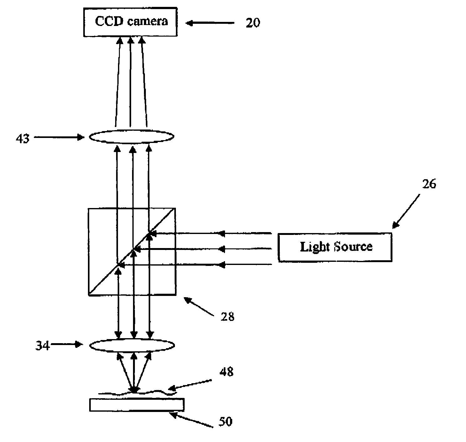
[0052] Interferometric techniques play an important role in the measurement of thin transparent films on substrates. The simplest interferometric method of measuring the thickness hfilm,(x,y) of a non-uniform thin film involves creating an image by superposition of beams reflected from two interfaces: air / film and film / substrate.
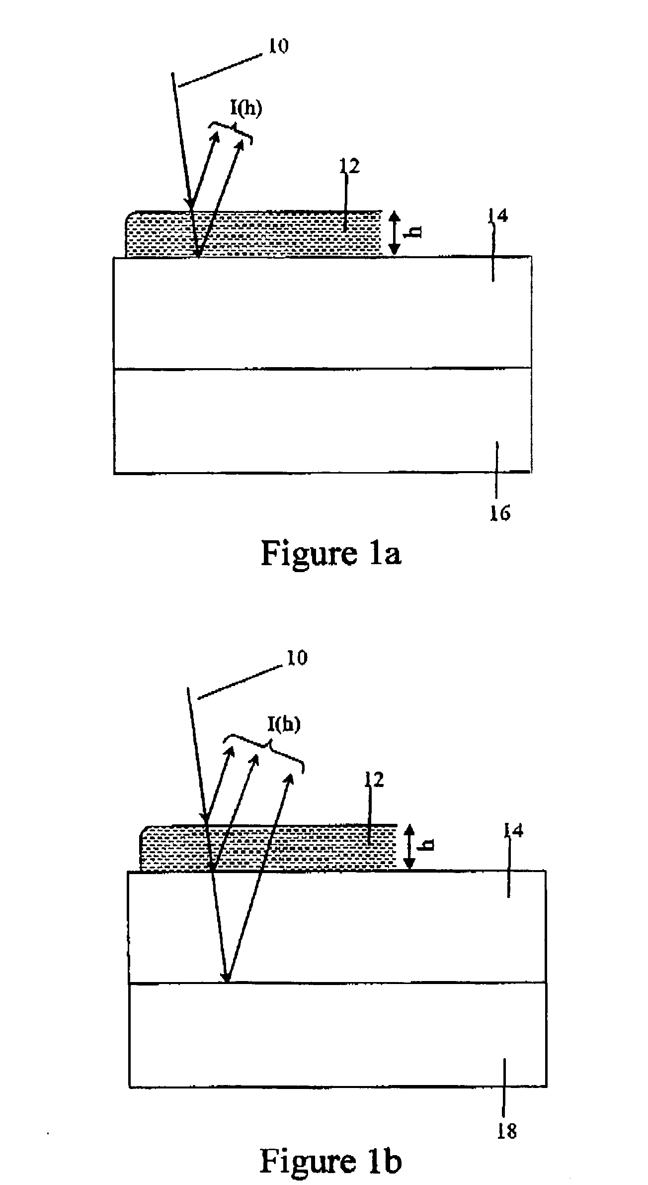
[0053]FIG. 1a illustrates two-beam interferometry for measuring the thickness of a thin water film 12 over a mica substrate 14. Incident light beam 10, which is either coherent or partially coherent with coherence length that is at least equal to the maximum thickness of the film (hereinafter—partially coherent), is directed onto thin film 12, and is partially reflected and partially refracted through. The refracted portion of the beam traverses through the thin film and then reflected by the water-mica interface. Absorbing grease 16 laid beneath mica substrate 14 is provided to inhibit reflections off the back surface of the mica substrate 14.
[0054] This ...
PUM
 Abstract
Description
Claims
Application Information