Driving circuit for optical modulator and method for driving optical modulator

a technology of optical modulator and driving circuit, which is applied in the direction of optics, transmission monitoring/testing/fault-measurement systems, instruments, etc., can solve the problems of light output waveform, increased costs, and transmission characteristics also deterioration

Inactive Publication Date: 2005-10-27
FUJITSU LTD
View PDF12 Cites 17 Cited by
  • Summary
  • Abstract
  • Description
  • Claims
  • Application Information

AI Technical Summary

Benefits of technology

[0016] Additionally, there is provided a driving method for an optical modulator, comprising the steps of: varying a pulse width of a data signal used for modulating input light; and adjusting a phase d...

Problems solved by technology

In order to keep up with recent high-speed transmission signals, such a conventional optical modulator, however, has to adjust a phase between the clock signal and the data signal with high accuracy because of a shortened time slot (for example, one time slot of a transmission signal of 40 Gb/s corresponds to 7.5 mm in a vacuum), resulting in increased costs.
Fluc...

Method used


Image

  • Driving circuit for optical modulator and method for driving optical modulator
  • Driving circuit for optical modulator and method for driving optical modulator
  • Driving circuit for optical modulator and method for driving optical modulator

Examples


first embodiment

[0044] [A] First Embodiment

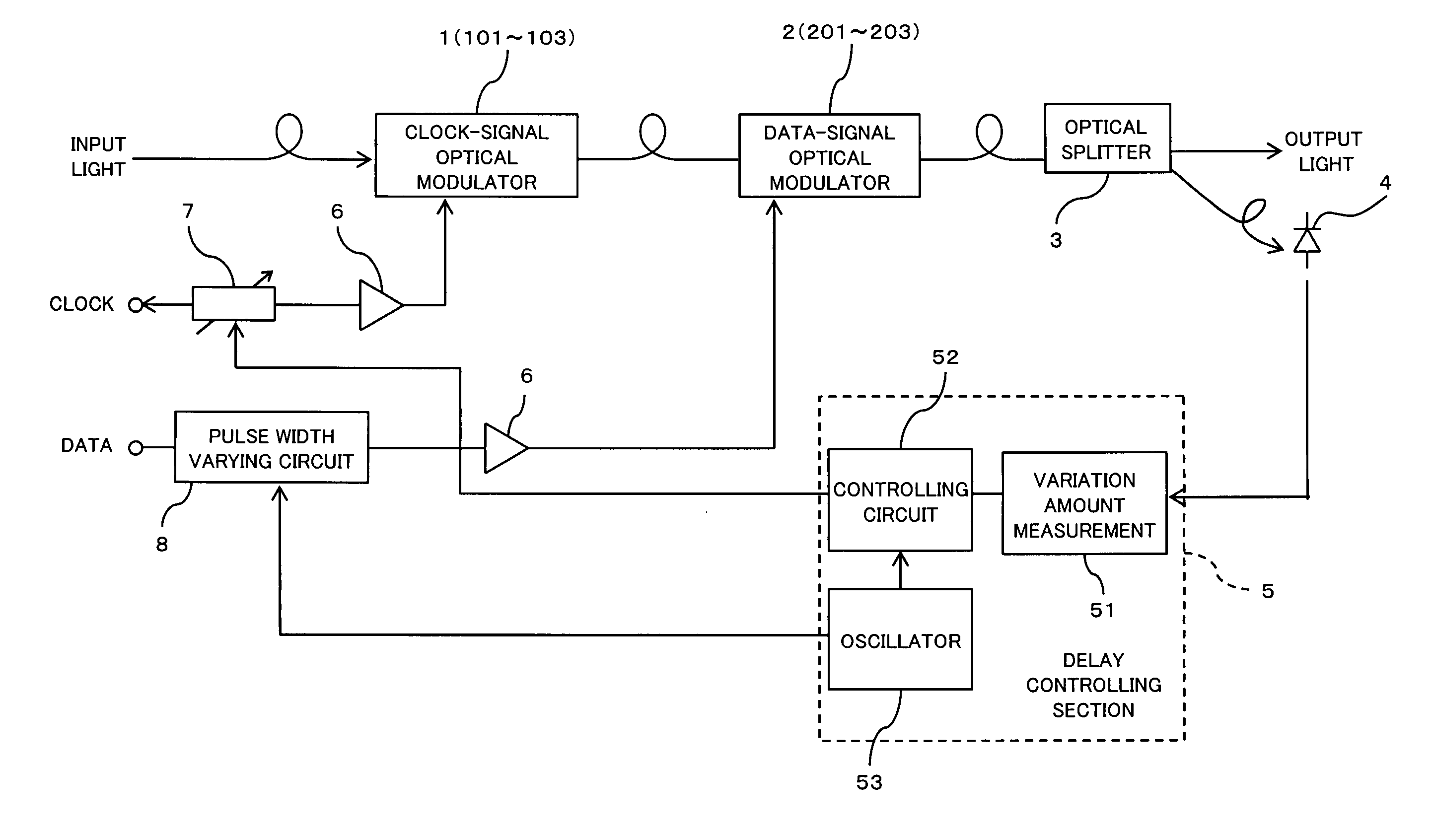
[0045]FIG. 1 is a block diagram schematically showing an optical modulator and the main part of a driving circuit thereof according to the first embodiment of the present invention. The optical modulator shown in FIG. 1 includes a Mach-Zehnder optical modulator (hereinafter called a clock modulator) 1 for a clock signal (CLK), a Mach-Zehnder optical modulator (hereinafter called a data modulator) for a data signal (DATA), and an optical splitter 3. The driving circuit includes a photodiode 4, a delay controlling section 5, amplifiers 6, a variable delay circuit 7 and pulse width varying circuit 8.

[0046] The clock modulator 1 and data modulator 2 are identical or similar to those explained above with reference to FIG. 18. The clock modulator 1 includes an input-side Y-shaped waveguide 101, electrodes 102 and an output-side Y-shaped waveguide 103, and modulates input light using a clock signal which is input to one of electrodes 102 through the variable del...

second embodiment

[0068] [B] Second Embodiment

[0069]FIG. 13 is a block diagram schematically showing an optical modulator and a main part of the driving circuit thereof according to a second embodiment of the present invention. The optical modulator shown in FIG. 13 has, as compared with that shown in FIG. 1, a controlling circuit 5A in substitution for the delay controlling section 5 and an electric-current / voltage (I / V) converting circuit 9, and is different in that it has no need for a variation amount measuring circuit 51 in the controlling circuit 5A and in installation of a pulse width setting circuit 54 from the delay controlling section 5. Other elements and parts with reference numbers already described are identical to or substantially identical to those described above.

[0070] Here, the pulse width setting circuit 54 fixedly sets a pulse width of a data signal supplied to the data modulator 2 to a width other than a standard pulse width in the pulse width varying circuit 8; and the I / V con...


PUM


Abstract

For an optical modulator for modulating input light using a clock signal and a data signal respectively, a pulse width varying circuit varies the pulse width of the data signal that is used for modulating the input light, and a delay control section carries out controls based on the light output power of the optical modulator in this state in such a manner that the phase difference between the clock signal and the data signal becomes minimum. As a result, it is possible to always adjust phases of the clock signal and the data signal to optimum phases and to stably obtain a fine light output waveform.

Description

CROSS REFERENCE TO RELATED APPLICATIONS [0001] This application is based on and hereby claims priority to International Application No. PCT / JP2002 / 013123 filed on Dec. 16, 2002 in Japan, the contents of which are hereby incorporated by reference. BACKGROUND OF THE INVENTION [0002] 1) Field of the Invention [0003] The present invention relates to a driving circuit for an optical modulator and a method for driving an optical modulator, and particularly relates to a driving circuit preferably for a Mach-Zehnder optical modulator that is used for an optical transmitter that transmits an RZ (Return to Zero) signal and a driving method therefor. [0004] 2) Description of the Related Art [0005] An accompanying drawing FIG. 18 is a block diagram schematically showing a conventional Mach-Zehnder optical modulator for generating an RZ signal and the main part of a driving circuit therefor. The Mach-Zehnder optical modulator shown in FIG. 18 is used in an optical transmitter that transmits an R...

Claims


Application Information

Patent Timeline
IPC IPC(8): G02F1/01H04B10/516H04B10/07H04B10/524H04B10/556H04B10/61
CPCH04B10/505H04B10/572H04B10/50577H04B10/5051
Inventor IKEUCHI, TADASHIKUWATA, NAOKI
Owner FUJITSU LTD
Why Eureka
Try Eureka