Method for printing an electronic circuit component on a substrate using a printing machine

a technology of electronic circuits and printing machines, applied in the direction of conductive pattern formation, lithography, instruments, etc., can solve the problems of easy destruction or removal of rfid tags printed on the exterior of packages, discoloration of printing substrates, and interference with the desired visual design of printed packages

Inactive Publication Date: 2005-11-03
MANROLANAD AG
View PDF10 Cites 6 Cited by
  • Summary
  • Abstract
  • Description
  • Claims
  • Application Information

AI Technical Summary

Benefits of technology

[0006] The present invention relates to a method for printing an electronic circuit or components thereof in a printing machine by the front-side printing and back-side printing method, where the conductive structure is printed on the printed front side of the printing substrate, the sheet is then reversed and the decorative printing motif or pattern is then printed on the back side in a single work step. As an alternative to the front-side and back-side printing method, the printed circuit can be printed by having the printing machines for color printing be preceded by a printing machine for printing on the back side of the printing substrate, so that the latter printing machine is turned from below against the advancing printing sheet. Furthermore, the patent describes a method for the application of a chip to the printing substrate without causing discoloration or damages to the printing substrate or the motif on the other side of the substrate.

Problems solved by technology

However, the printed antennas can interfere with the desired visual design of the printed package, because of the color hue of the conductive printing inks and its relatively high layer density, which is required to achieve good conductivity of the seams.
In addition, the RFID tag which is printed on the exterior of a package can be destroyed or removed easily.
An additional problem arises if, in a later processing step, the chip is glued or soldered to the contact place of the antenna.
During the adhesive process or soldering process, heat is often generated at the adhesion places, causing discoloration of the printing substrate or, in a worse case, burns on the printing substrate.
The discoloration or burns are not desired if only because they interfere with the decorative appearance of the packages.

Method used


Image

  • Method for printing an electronic circuit component on a substrate using a printing machine
  • Method for printing an electronic circuit component on a substrate using a printing machine
  • Method for printing an electronic circuit component on a substrate using a printing machine

Examples


Embodiment Construction

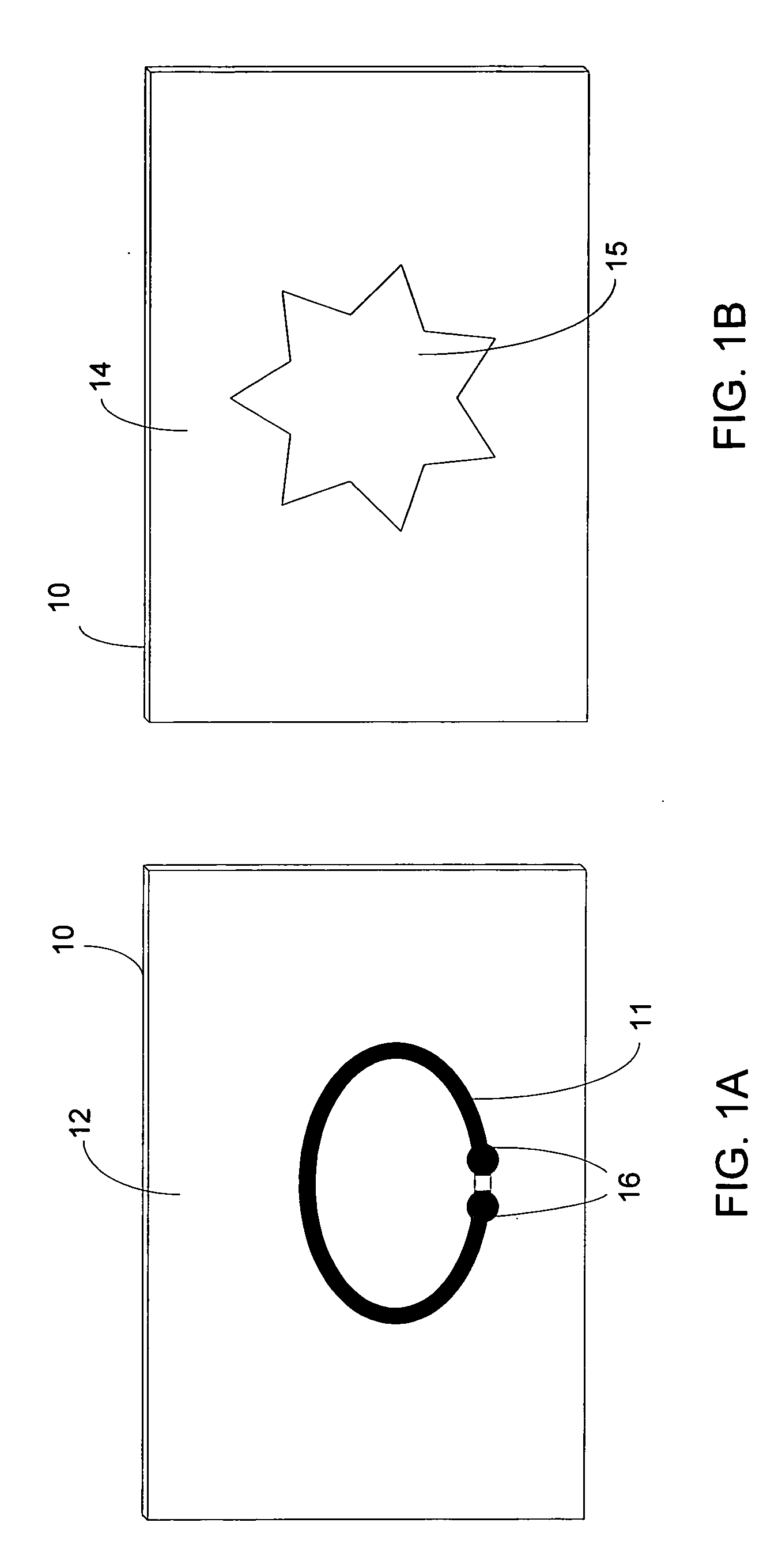
[0012]FIGS. 1A and 1B show a highly simplified example of a sheet-like substrate 10 that has a conductive structure printed thereon to form a component 11 of an electronic circuit. The component 11 may be, for example, an coil that serves as the antenna for an RFID circuit. For such an application, the ends of the coil may have contact patches 16 for attaching to a RFID chip. The component 11 is printed on one side, such as the backside 12, of the printed substrate 10, while the opposite side of the substrate, in this example the front side 14, has a design or pattern 15, such as decorative motif, printed thereon.

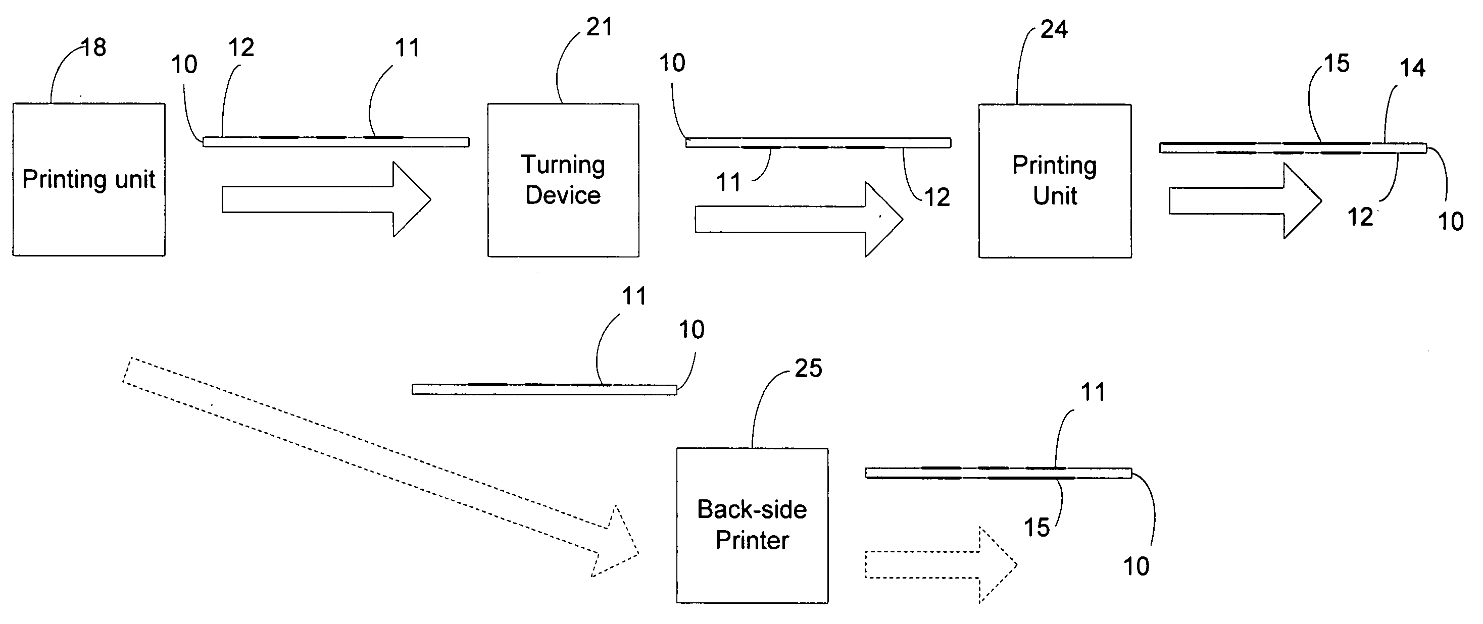
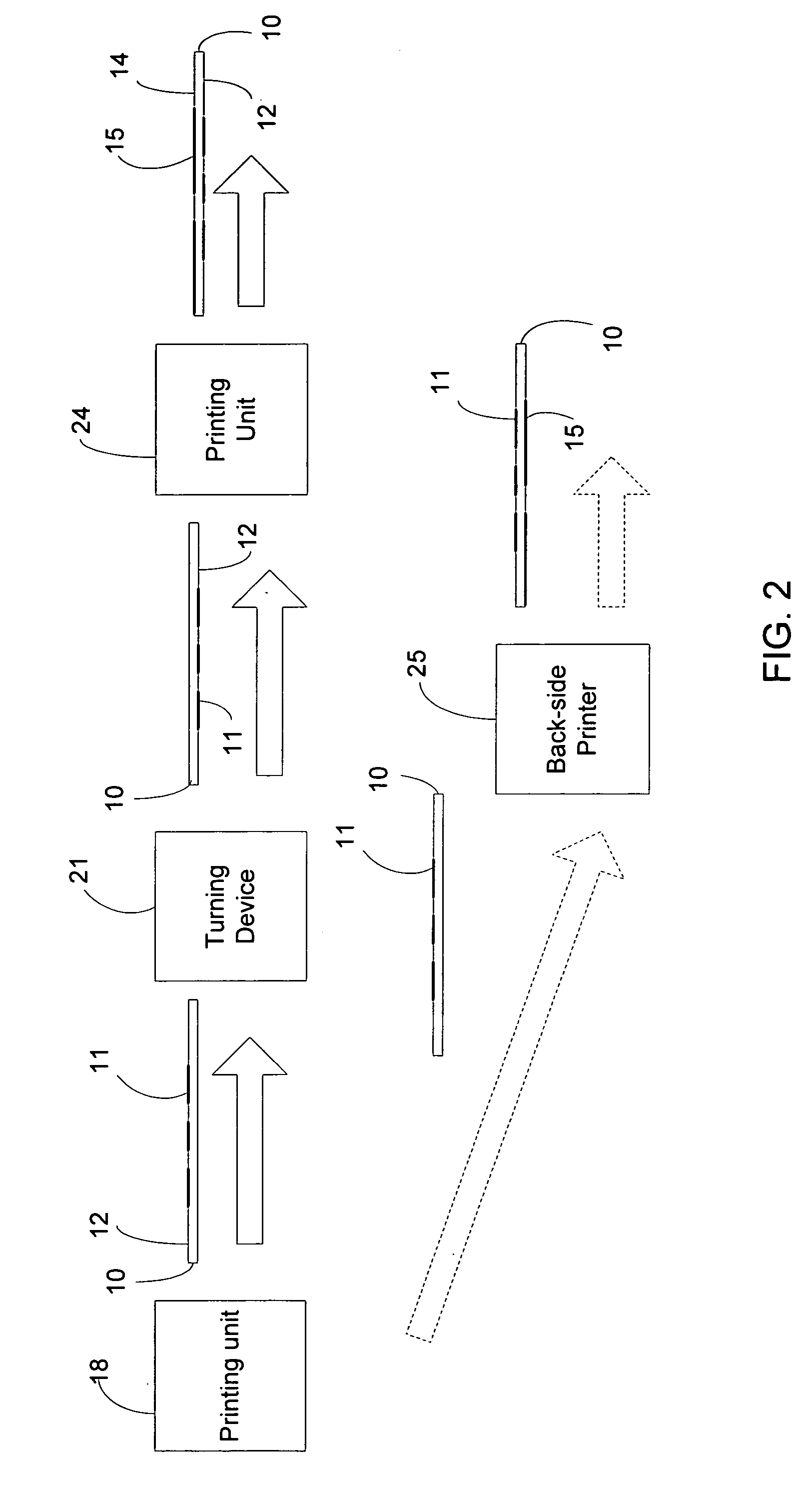
[0013] According to the invention, the problem of the prior art described earlier is solved by printing parts of the circuit on the inner side of the package (front printing side or back side of the sheet of the printing substrate using the S & W method). As shown in FIG. 2, the circuit part or component 11 is printed using one printing unit 18 of the printing system 20. T...


PUM


Abstract

A method of printing an electronic circuit or components thereof uses a printing machine to print a conductive structure on the front printing side (back side of the sheet) of a printing substrate. The sheet is then reversed and a decorative printing motif is printed on the back side in one work step. Alternatively, the circuit or components of a circuit may be printed by having a printing machine for color printing preceded by a printing machine for printing on the back side of the printing substrate. A chip is applied to the printing substrate where the back side of the printing sheet with the printing motif is cooled to prevent any negative effect on the printing motif and / or the printing substrate.

Description

FIELD OF THE INVENTION [0001] The invention relates to methods of forming a printed electronic circuit, and more particularly to printing an electronic circuit component onto a substrate using a printing machine. BACKGROUND OF THE INVENTION [0002] Conductive materials are often applied to a circuit board substrate using the screen printing technique. A conductive paste, which can contain, for example, silver, aluminum or conductive carbon black, is applied to a substrate to produce a conductor on the substrate. Applications are also known in which similar conductive printing methods are applied to a printing substrate in a lithographic printing method. [0003] One of the possible applications is the so called radio frequency identification (RFID) tags. These RFID tags present the possibility of storing data on a product. The stored data can be used, for example, to control product streams and simplify the management of inventories. Because of the clearly higher data storage capacity ...

Claims


Application Information

Patent Timeline
Patent Type & Authority Applications(United States)
IPC IPC(8): G06K19/07B41M3/00G06K19/077H05K1/02H05K3/04H05K3/12
CPCG06K19/07749H05K1/0266H05K3/046H05K3/12H05K2203/1581H05K2203/0522H05K2203/0534H05K2203/1563H05K3/1275
Inventor WALTHER, THOMAS
Owner MANROLANAD AG
Why Eureka
Try Eureka