

Thin lightshield process for solid-state image sensors
a technology of solid-state image sensors and lightshields, applied in the direction of material analysis, instruments, radiation control devices, etc., can solve the problems of degrading performance, corrosion of these films, electrical properties or optical light-shielding properties, etc., and achieve the effect of thin lightshields and minimizing corrosion of aluminum and tiw layers
- Summary
- Abstract
- Description
- Claims
- Application Information
AI Technical Summary
Benefits of technology
Problems solved by technology
Method used
Image

Examples
Embodiment Construction
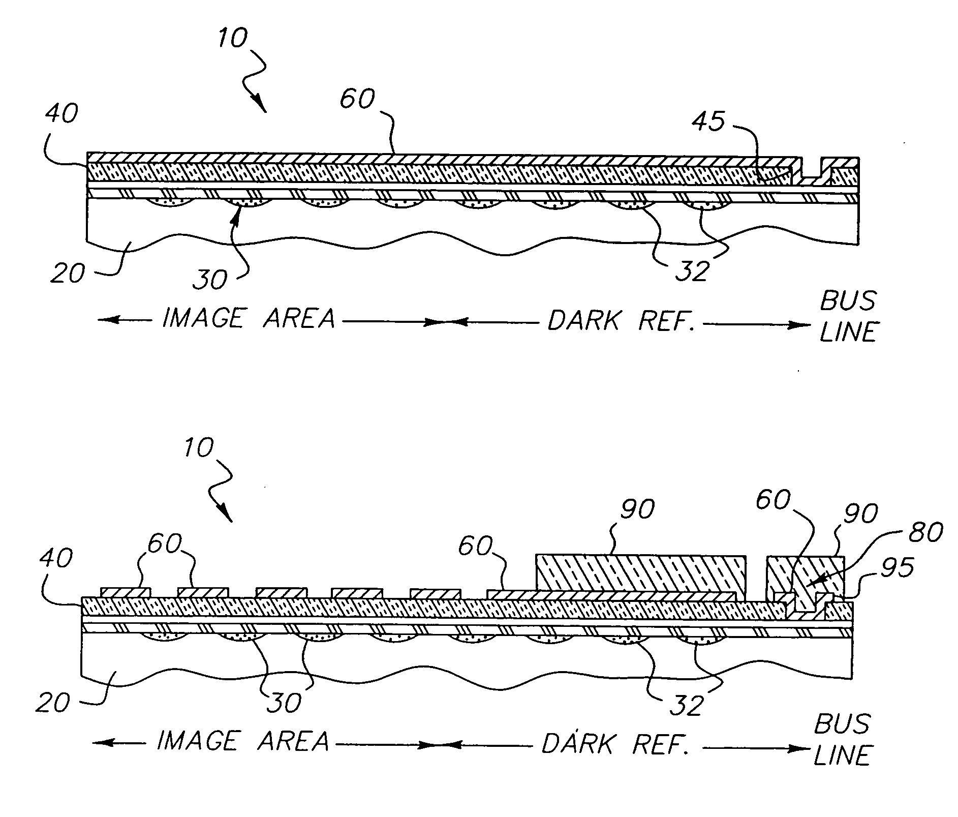
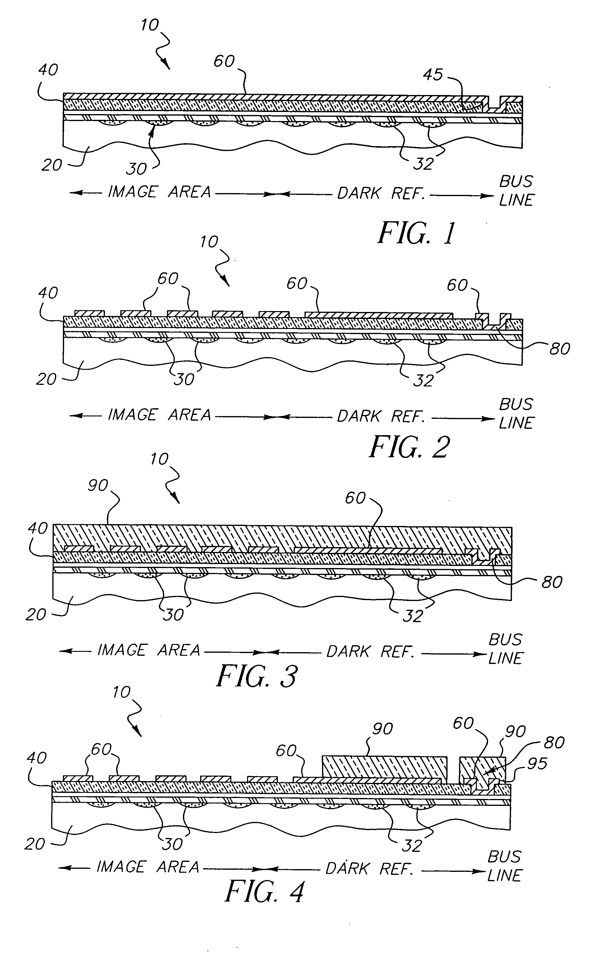
[0016] Referring to FIG. 1, a typical image sensor 10 consists of an array of photosensitive elements or pixels 30 in an image area. Within each pixel are regions that are exposed to light so that an electrical signal may be created in response to the incident light. In addition, there are regions within the pixel, which are prevented from receiving light because the light will degrade the imaging performance. A typical image sensor 10 also provides dark reference pixels 32 that are insensitive to light because they are covered with a light shield.
[0017] The signal from these dark reference pixels 32 are used in the signal processing portion of the camera to indicate the signal of photosensitive pixels when no light is incident upon them. In addition, interconnects are provided within the image sensor to electrically connect various parts of the imager and to provide means to connect the imager to external circuits.
[0018] Referring to FIG. 1, there is shown an initial stage of for...
PUM
 Abstract
Description
Claims
Application Information