Memory module, socket and mounting method providing improved heat dissipating characteristics

a memory module and socket technology, applied in the direction of final product manufacturing, coupling device connection, sustainable manufacturing/processing, etc., can solve the problems of extremely poor thermal conductivity of air, unexpected increase of inferior refresh rate, etc., to reduce factors liable to be barriers to dissipating heat from semiconductor devices mounted on memory modules, and reduce air gaps. , the effect of reducing factors

Active Publication Date: 2005-11-03
SAMSUNG ELECTRONICS CO LTD
View PDF8 Cites 8 Cited by
  • Summary
  • Abstract
  • Description
  • Claims
  • Application Information

AI Technical Summary

Benefits of technology

[0025] According to the present invention, structures of a memory module and a socket may reduce and/or eliminate an air gaps that may otherwise exist between the socket and the memory module. Therefore, factors liable to be a barrier to dissipating heat from a semiconductor device mounted on the memory

Problems solved by technology

For example, a refresh characteristic of a DRAM memory module may degraded at a temperature of 80° C. and higher, which may unexpe

Method used


Image

  • Memory module, socket and mounting method providing improved heat dissipating characteristics
  • Memory module, socket and mounting method providing improved heat dissipating characteristics
  • Memory module, socket and mounting method providing improved heat dissipating characteristics

Examples


Embodiment Construction

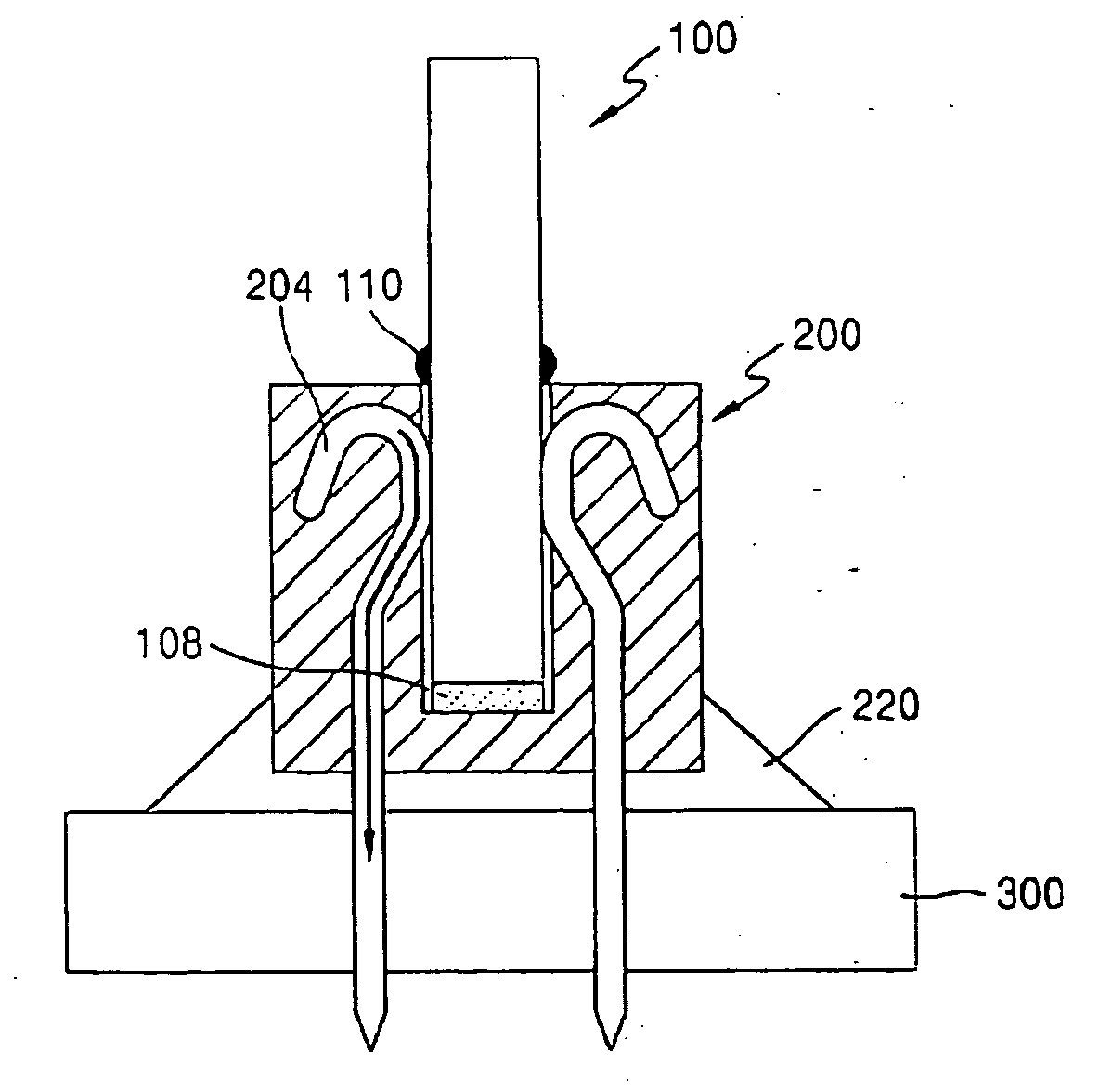
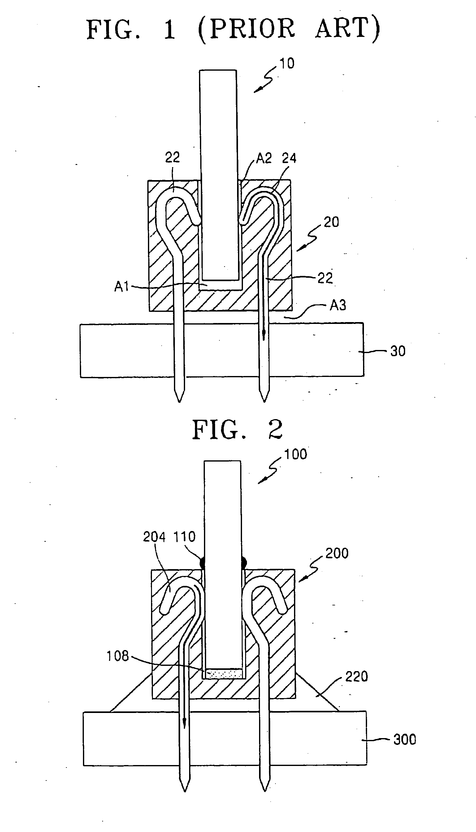
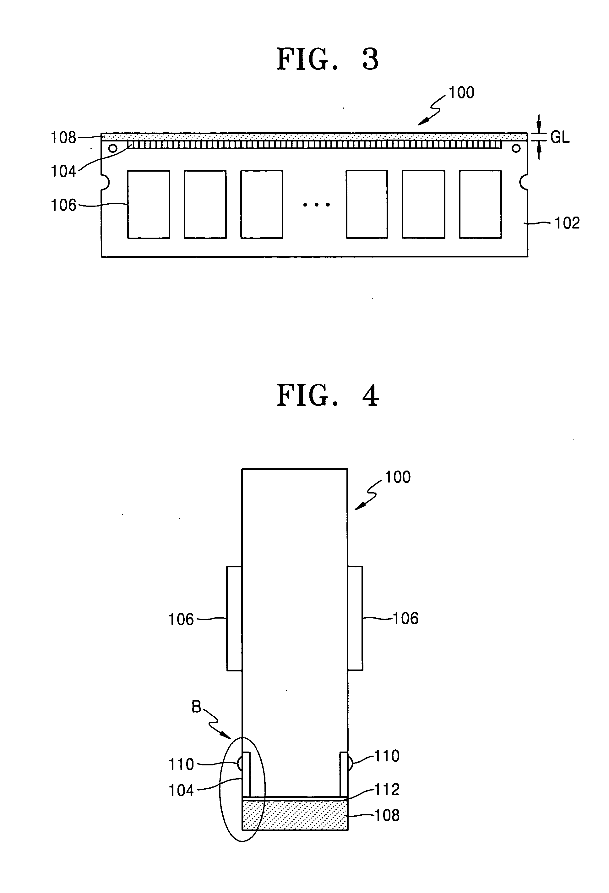
[0042] Exemplary, non-limiting embodiments of the present invention will now be described more fully with reference to the accompanying drawings. The invention may, however, be embodied in many different forms and should not be construed as being limited to the embodiments set forth herein; rather these embodiments are provided so that this disclosure will be thorough and complete, and will fully convey the concept of the invention to those skilled in the art. The principles and features of this invention may be employed in varied and numerous embodiments without departing from the scope of the invention.

[0043] In this disclosure, well-known structures and processes may not be described or illustrated in detail to avoid obscuring the present invention. Furthermore, the figures are not drawn to scale. Rather, for simplicity and clarity of illustration, the dimensions of some of the elements may be exaggerated relative to other elements. A layer may be considered as being formed (or ...


PUM


Abstract

In a memory module, a gap filler for eliminating an air gap may be formed on an end of a PCB where a tab may be formed. The gap filler may be formed on a surface of a socket receiving the memory module. A grease may be coated on the tab to provide a heat conduction path away from the memory module.

Description

BACKGROUND OF THE INVENTION [0001] This application claims the benefit of priority of Korean Patent Application No. 2004-22027, filed on Mar. 31, 2004, in the Korean Intellectual Property Office, the disclosure of which is incorporated herein in its entirety by reference. [0002] 1. Field of the Invention [0003] The present invention relates generally to a semiconductor device, a socket for mounting the semiconductor device and a semiconductor device mounting method, and more particularly to a memory module, a socket and a mounting method. [0004] 2. Description of the Related Art [0005] Semiconductor devices such as DRAMs (for example) may be implemented in a memory module. A memory module may have a plurality of semiconductor devices that may be mounted on a printed circuit board. An electrical characteristic of a DRAM device may be refresh characteristics, which may deteriorate at elevated temperatures. Thus, it may be advantageous to dissipate heat generated from a memory module. ...

Claims


Application Information

Patent Timeline
IPC IPC(8): H01L23/50H01R13/62H05K3/30
CPCH05K3/305H05K3/306H05K2201/0133H01R12/721H05K2201/10446H05K2203/1147H05K2203/304H05K2201/10189Y02P70/50H01L23/50
Inventor PARK, SANG-WOOKBAEK, JOONG-HYUNLEE, HAE-HYUNGCHOI, HEE-KOOKLEE, JIN-YANG
Owner SAMSUNG ELECTRONICS CO LTD
Why Eureka
Try Eureka