Display device

Inactive Publication Date: 2005-11-10
MITSUBISHI ELECTRIC CORP
View PDF7 Cites 29 Cited by
  • Summary
  • Abstract
  • Description
  • Claims
  • Application Information

AI Technical Summary

Benefits of technology

[0006] In view of the foregoing problems, it is an object of the present invention to provide a display device that mak

Problems solved by technology

However, in this case, with methods that involve the placement of TCPs or driver circuits on extending lines of the drive signal lines of the display region as per the prior art, there have been problems such as the great complicat

Method used


Image

  • Display device
  • Display device
  • Display device

Examples


first embodiment

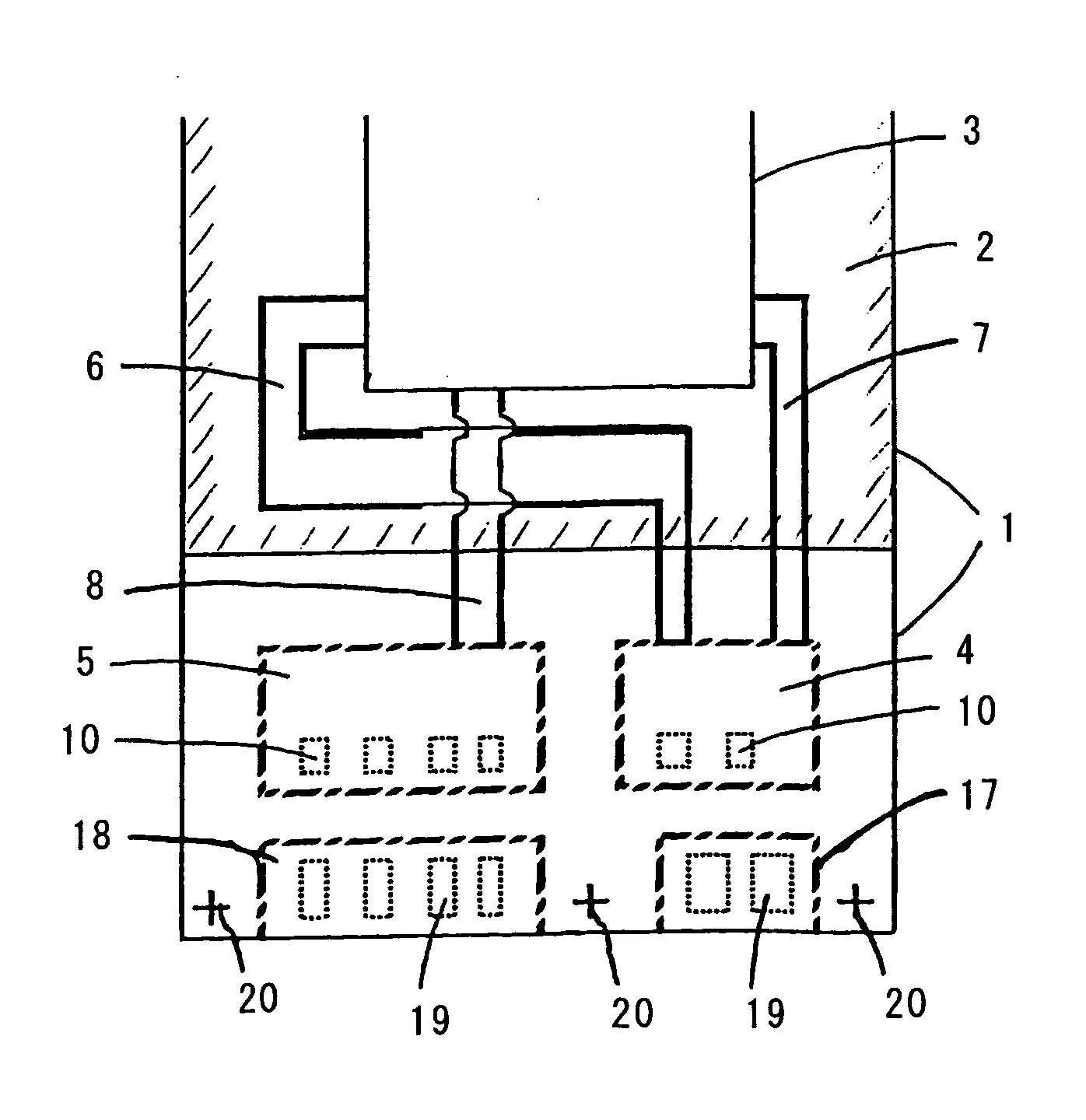
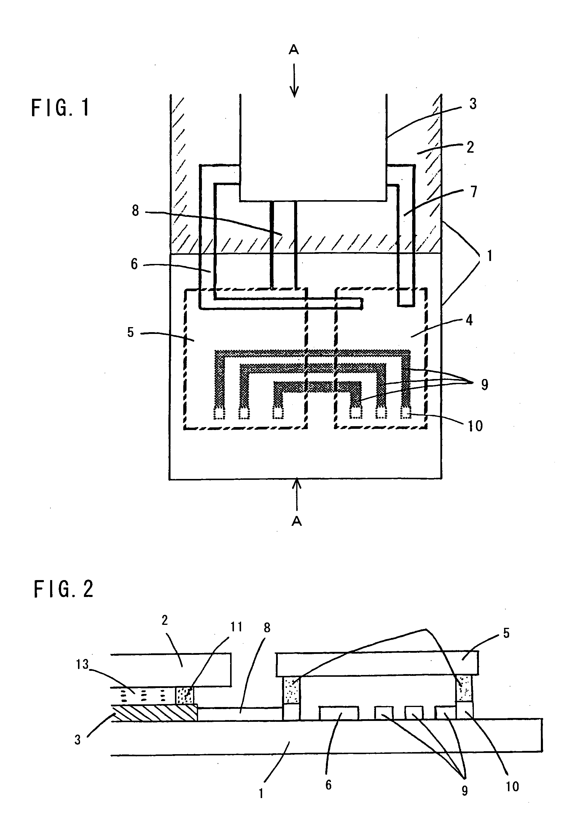
[0032] A first embodiment of the present invention will be described by means of FIGS. 1 and 2. FIG. 1 is a planar view of the liquid crystal display device according to the first embodiment of the present invention, and FIG. 2 is a cross-section along the line A-A in FIG. 1.

[0033] In FIGS. 1 and 2, 1 denotes an insulating substrate constituted by a glass substrate, for example; 2 denotes an opposing substrate; 3 denotes a display region that comprises pixel electrodes, and so forth; 4 denotes a scan line driver circuit; 5 denotes a signal line driver circuit; 6 denotes a group of lines that connects scan lines on one side of the display region and a scan line driver circuit; 7 denotes a group of lines that connects scan lines on a side that lies opposite to the one side of the display region and the scan line driver circuit; 8 denotes a group of lines that connects the signal lines of the display region and the signal line driver circuit; 9 denotes connecting lines that connects t...

second embodiment

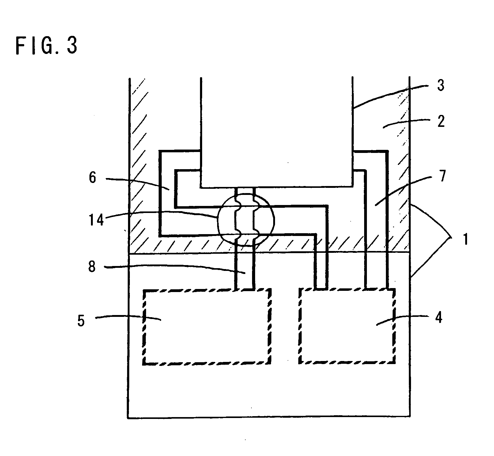
[0036] The second embodiment of the present invention will now be described by referring to FIG. 3. FIG. 3 is a planar view of the liquid crystal display device of the second embodiment of the present invention. In FIG. 3, the same reference numerals is assigned to constituent parts which are the same as those in FIGS. 1 and 2, and a description is therefore provided with respect to the differences. In FIG. 3, 14 denotes crossover points between the group of scan lines 6 and the group of signal lines 8. In the present embodiment, unlike the constitution as in the first embodiment above in which at least a part of the group of scan lines, which is connected to one side of the display region, is formed in a region on the insulating substrate in which the signal line driver circuit is mounted, the group of scan lines 6 and the group of signal lines 8 are formed so as to intersect at the crossover points 14 in a region of overlap between the insulating substrate 1 and the opposing subst...

third embodiment

[0038] The third embodiment of the present invention will now be described by means of FIG. 4. FIG. 4 is a planar view of the liquid crystal display device according to the third embodiment of the present invention. In FIG. 4, the same reference numerals are assigned to constituent parts which are the same as those of FIGS. 1 to 3, and therefore a description will be provided with respect to the. differences. In FIG. 4, 15 denotes transfer electrodes for supplying an opposite potential (common potential) to the opposing substrate, and 16 is common potential supply wiring for supplying an opposite potential (common potential) to the transfer electrodes 15. As shown in FIG. 4, the present embodiment is such that wiring such as the group of scan lines 6 and 7 and the group of signal lines 8 is not present, and hence the transfer electrodes 15, which supply an opposite potential (common potential) from outside the liquid crystal panels to the opposing substrate via a driver circuit are ...


PUM


Abstract

A display device comprises scan lines on a insulating substrate, signal lines intersecting with the scan lines with an insulating film interposed therebetween, a display area comprising pixel electrodes connected to the signal lines, a scan line driver circuit connected to the scan lines, a signal line driver circuit connected to the signal lines. The scan line driver circuit and the signal line driver circuit are mounted directly on the insulating substrate outside of the display area and close to one side of the display area. Lines connecting the scan line driver circuit and the signal line driver circuit are formed in an area in which the scan line driver circuit and the signal line driver circuit are mounted.

Description

BACKGROUND OF THE INVENTION [0001] 1 . Field of the Invention [0002] The present invention relates to a display device which is driven by driver circuits and more particularly to a preferred display device that is applied to a liquid crystal display device. [0003] 2 . Related Background Art [0004] Display devices which are employed in conventional liquid crystal display monitor devices or notebook computers and the like require a display pixel count of 480×640 even for a small VGA (Video Graphic Array) mode display device, and require drive signal lines pertaining to several hundred levels. Where active matrix drive-type display devices are concerned, a plurality of respective driver circuits is needed to drive the sources or gates of the thin film transistors. Accordingly, the driver circuits or TCPs (Tape Carrier Packages) which afford a connection to the driver circuits are disposed on extending lines on the same side of the drive signal lines within the display region. [0005] In...

Claims


Application Information

Patent Timeline
IPC IPC(8): G02F1/13G02F1/1333G02F1/1345G09F9/00G09F9/30G09G3/20G09G3/36
CPCG02F1/133351G02F2001/133354G02F1/13452G02F1/1345G02F1/133354
Inventor HIROSUE, MIYUKINAKAYAMA, AKIO
Owner MITSUBISHI ELECTRIC CORP
Why Eureka
Try Eureka