Solid-state imaging device, method for producing solid-state imaging device, and electronic apparatus using photoelectric conversion elements

a technology of solid-state imaging and electronic equipment, which is applied in the direction of color television, television system, radio control devices, etc., can solve the problems of difficult high-speed transfer, suppress white flaws and another deterioration of pixel characteristics, and reduce the difficulty of high-speed reading

Active Publication Date: 2019-04-16
BRILLNICS JAPAN
View PDF34 Cites 2 Cited by
  • Summary
  • Abstract
  • Description
  • Claims
  • Application Information

AI Technical Summary

Benefits of technology

[0031]According to the present invention, high speed reading becomes possible using a small chip area. In addition, there is little restriction in layout, and it becomes possible to suppress white flaws and another deterioration of pixel characteristics. Further, according to the present invention, it becomes possible to form a pixel portion by a CCD process having a good dark current characteristic. Further, miniaturization of pixels for global shutter becomes possible. Further, according to the present invention, a drive interface can be simplified. Further it is also possible to eliminate the horizontal CCD, therefore reduction of the consumed power becomes possible. Further, according to the present invention, increase of functions such as digital output conversion and on-chip signal processing becomes possible.

Problems solved by technology

This IT type CCD image sensor 1 has a structure enabling progressive reading (progressive scanning), but transfers the signal charges by the horizontal CCD 3, so high speed transfer is difficult.

Method used


Image

  • Solid-state imaging device, method for producing solid-state imaging device, and electronic apparatus using photoelectric conversion elements
  • Solid-state imaging device, method for producing solid-state imaging device, and electronic apparatus using photoelectric conversion elements
  • Solid-state imaging device, method for producing solid-state imaging device, and electronic apparatus using photoelectric conversion elements

Examples


first embodiment

[0074]FIG. 5 is a view showing an example of the configuration of a solid-state imaging device according to a first embodiment of the present invention spread out flat. FIG. 6 is a view schematically showing a first example of a stacked substrate structure of the solid-state imaging device according to the present embodiment. FIG. 7 is a view schematically showing a second example of the stacked substrate structure of the solid-state imaging device according to the present embodiment. FIG. 8 is a view for explaining the relationship of arrangement between a photosensitive part on the first substrate and a peripheral circuit part on the second substrate which are stacked in the solid-state imaging device according to the first embodiment.

[0075]The solid-state imaging device 100 can be applied to an image sensor similar to for example an FIT (frame interline transfer) type CCD image sensor. However, the present solid-state imaging device 100 does not have the charge storage part (stor...

second embodiment

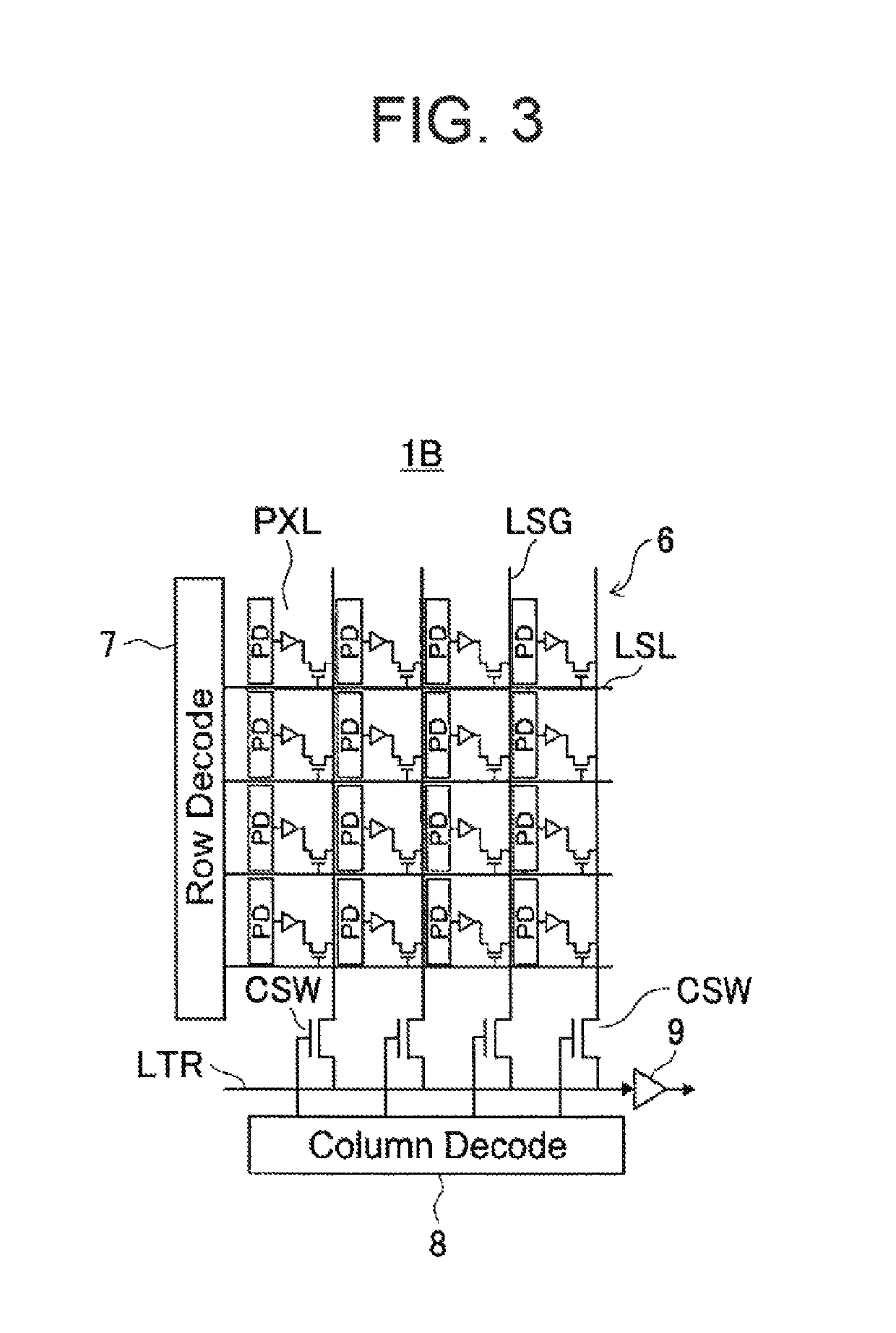
[0152]FIG. 23 is a view for explaining an example of the configuration of a solid-state imaging device according to a second embodiment of the present invention.

[0153]The difference of a solid-state imaging device 100K according to the second embodiment from the solid-state imaging device 100 in the first embodiment explained above is as follows. The solid-state imaging device 100K in the second embodiment includes a relay selecting part 250 which selectively connects a plurality of vertical transfer parts 212-1 to 212-4 and the conversion / output part 220 (and connecting part 231).

[0154]In the second embodiment, a plurality of selection electrodes 251-1, 251-2, 251-3, and 251-4 are arranged on the first substrate 110K. Further, on the first substrate 110K and second substrate 120K, one common conversion / output part 220K and through-via (TSV) 140K as the connecting part are formed for a plurality of selection electrodes 251-1 to 251-4.

[0155]In FIG. 23, at the through-via 140K on the ...

third embodiment

[0181]FIG. 27 is a view for explaining an example of the configuration of a solid-state imaging device according to a third embodiment of the present invention.

[0182]The difference of a solid-state imaging device 100O according to the third embodiment from the solid-state imaging device 100 in the first embodiment explained above is as follows. In the solid-state imaging device 100O according to the third embodiment, on the second substrate 120O, the ADC 341, serializer 342, memory 343, and timing generator (TG) 344 of the signal processing system comprised of the peripheral circuit part 300O are formed. The timing generator (TG) 344 includes a CCD pulse driving part and level shift etc.

[0183]Here, using a CMOS image sensor as a comparative example, the chip sizes of a CCD image sensor and a CMOS image sensor used as the solid-state imaging device 100O according to the third embodiment mounting the signal processing system on the second substrate 120O will be considered.

[0184]FIGS. ...


PUM


Abstract

A solid state imaging device has: a photosensitive part containing a plurality of charge transfer parts that transfer, in column units, the signal charges of a plurality of photoelectric conversion elements disposed in a matrix; a conversion / output unit that converts, to an electrical signal, the signal charges forwarded by the charge transfer parts; a peripheral circuit part that performs a predetermined process with respect to the electrical signals from the conversion / output part; a relay part that relays the forwarding to the peripheral circuit part of the electrical signal from the conversion / output part; a first substrate where a photosensitive part and the conversion / output part are formed; and a second substrate where the peripheral circuit part is formed. The first and second substrates are stacked together, and the relay part electrically connects the conversion / output part formed at the first substrate to the peripheral circuit part formed at the second substrate.

Description

TECHNICAL FIELD[0001]The present invention relates to a solid-state imaging device using a photoelectric conversion element which detects light and generates a charge, a method for producing a solid-state imaging device, and an electronic apparatus.BACKGROUND ART[0002]As a solid-state imaging device (image sensor) using a photoelectric conversion element which detects light and generates a charge, a CCD (charge coupled device) image sensor and CMOS (complementary metal oxide semiconductor) image sensor have been put to practical use. CCD image sensors and CMOS image sensors are widely applied as portions of digital cameras, video cameras, monitoring cameras, medical endoscopes, personal computers (PC), mobile phones and other portable terminal devices (mobile devices), and other various types of electronic apparatuses.[0003]A CCD image sensor and CMOS image sensor use photodiodes for the photoelectric conversion elements, but differ in methods of transferring photoelectrically conve...

Claims


Application Information

Patent Timeline
Patent Type & Authority Patents(United States)
IPC IPC(8): H04N5/378H04N5/372H04N5/369H04N5/374H01L27/146H01L27/148
CPCH04N5/378H04N5/379H01L27/1469H01L27/1485H01L27/14623H01L27/14634H01L27/14636H01L27/14643H01L27/14689H01L27/14812H01L27/14818H01L27/14887H04N5/372H04N5/374H01L27/1464H04N25/70H04N25/79H04N25/76H04N25/75H04N25/71
Inventor TAKAYANAGI, ISAOTANAKA, SHUNSUKEMORI, KAZUYAARIYOSHI, KATSUHIKOMATSUO, SHINICHIRO
Owner BRILLNICS JAPAN
Why Eureka
Try Eureka