Method of forming fin field effect transistor using damascene process

a damascene and fin field technology, applied in the field of damascene process, can solve the problems of difficulty in further scaling down transistors and various problems,

Active Publication Date: 2005-11-17
SAMSUNG ELECTRONICS CO LTD
View PDF10 Cites 38 Cited by
  • Summary
  • Abstract
  • Description
  • Claims
  • Application Information

AI Technical Summary

Benefits of technology

[0016] In some embodiments, the filling insulation pattern is recessed using a wet etch. Prior to formation of the gate insulation layer, the method may further comprise trimming, at least once, the channel portion of the fin to cont

Problems solved by technology

However, the short channel effect or drain induced barrier lower (DIBL) phenomenon makes it difficult to scale down tran

Method used


Image

  • Method of forming fin field effect transistor using damascene process
  • Method of forming fin field effect transistor using damascene process
  • Method of forming fin field effect transistor using damascene process

Examples


Embodiment Construction

[0021] The invention will be described below with reference to the accompanying drawings, in which embodiments of the invention are shown. The invention may, however, be embodied in many different forms and should not be construed as limited to the embodiments set forth herein. Rather, these embodiments are provided so that this disclosure will be thorough and complete, and will fully convey the scope of the invention to those skilled in the art. In the drawings, the thicknesses of layers and regions are exaggerated for clarity. It will be understood that when a layer is referred to as being “on” another element, it can be directly on the element or intervening elements may also be present. Like reference numerals refer to similar or identical elements throughout.

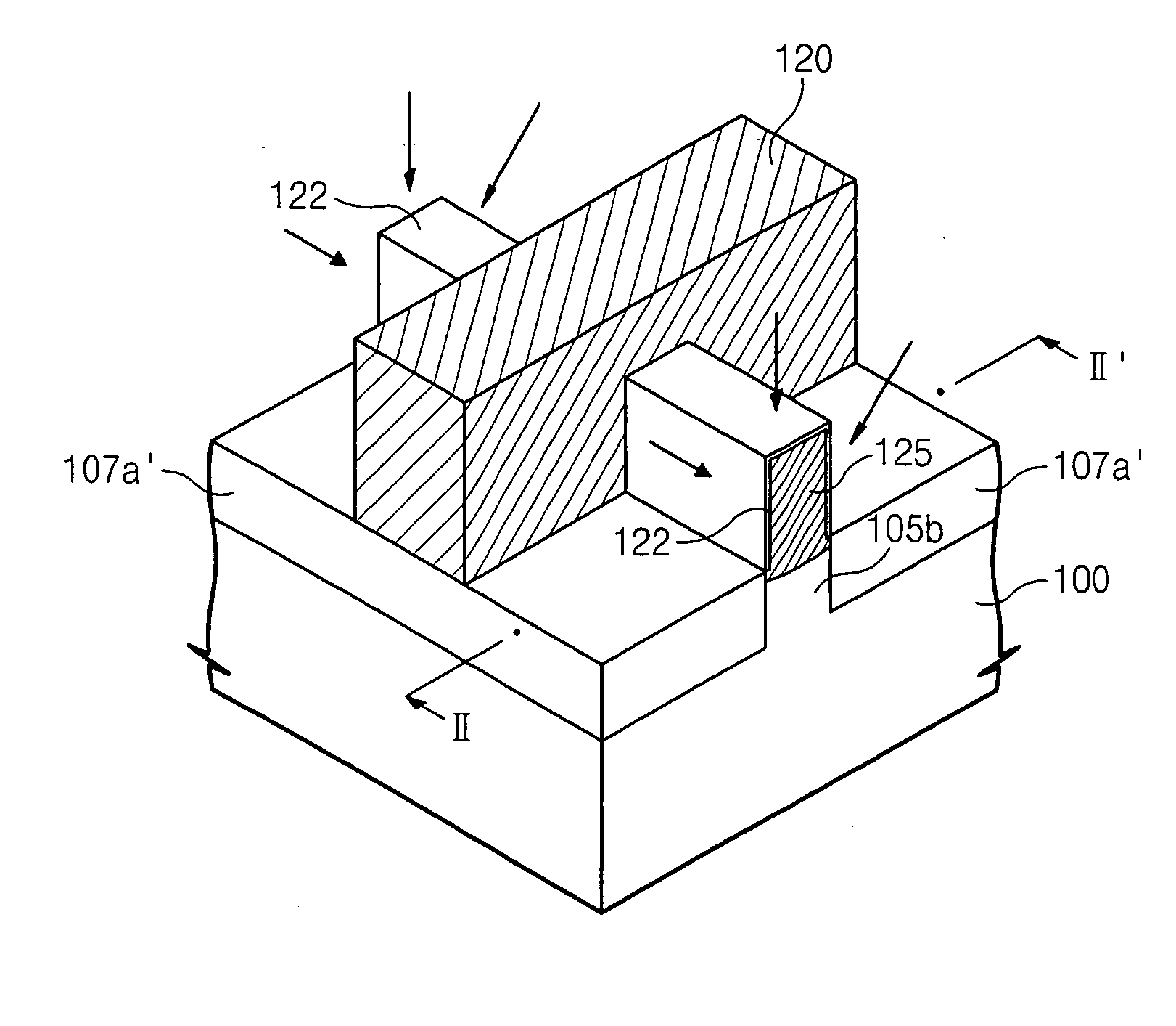
[0022] As illustrated in FIG. 4A and FIG. 4B, a hard mask pattern 102 is formed on a predetermined region of a substrate 100. The substrate 100 is etched to form a vertically protruding fin 105, using the hard mask pattern...


PUM


Abstract

A method of forming a fin transistor using a damascene process is provided. A filling mold insulation pattern is recessed to expose an upper portion of a fin, and a mold layer is formed. The mold layer is patterned to form a groove crossing the fin and exposing a part of the upper portion of the fin. A gate electrode is formed to fill the groove with a gate insulation layer interposed between the fin and the gate electrode, and the mold layer is removed. Impurities are implanted through both sidewalls and a top surface of the upper portion of the fin disposed at opposite sides of a gate electrode to form a source/drain region.

Description

CROSS-REFERENCE TO RELATED APPLICATIONS [0001] This application claims priority from Korean Patent Application No. 2004-34352, filed on May 14, 2004 in the Korean Intellectual Property Office, the disclosure of which is incorporated herein by reference in its entirety. BACKGROUND OF THE INVENTION [0002] 1. Field of the Invention [0003] The invention relates to a method of forming a semiconductor device and, more particularly, to a method of forming a fin field effect transistor using a damascene process. [0004] 2. Description of Related Art [0005] With the recent trend toward smaller semiconductor devices, field effect transistors of semiconductor devices (hereinafter referred to as “transistors”) have been scaled down. However, the short channel effect or drain induced barrier lower (DIBL) phenomenon makes it difficult to scale down transistors further. In view of the foregoing, fin transistors have been proposed. A typical fin transistor includes a fin vertically protruding from a...

Claims


Application Information

Patent Timeline
IPC IPC(8): H01L21/265H01L21/336H01L21/8234H01L29/78H01L21/8242H01L29/786
CPCH01L21/26586H01L29/7851H01L29/66818E02B3/14A01G9/02
Inventor AHN, YOUNG-JOONPARK, DONG-GUNLEE, CHOONG-HOKANG, HEE-SOO
Owner SAMSUNG ELECTRONICS CO LTD
Why Eureka
Try Eureka