Hydrogen sensor and method for detecting hydrogen
- Summary
- Abstract
- Description
- Claims
- Application Information
AI Technical Summary
Benefits of technology
Problems solved by technology
Method used
Image
Examples
first embodiment
[0049] Next, an embodiment of a hydrogen sensor according to the present invention will be described with reference to figures.
[0050] In all the following figures, in order to facilitate understanding thereof, the film thicknesses and dimensional ratios of individual constituent elements are optionally changed.
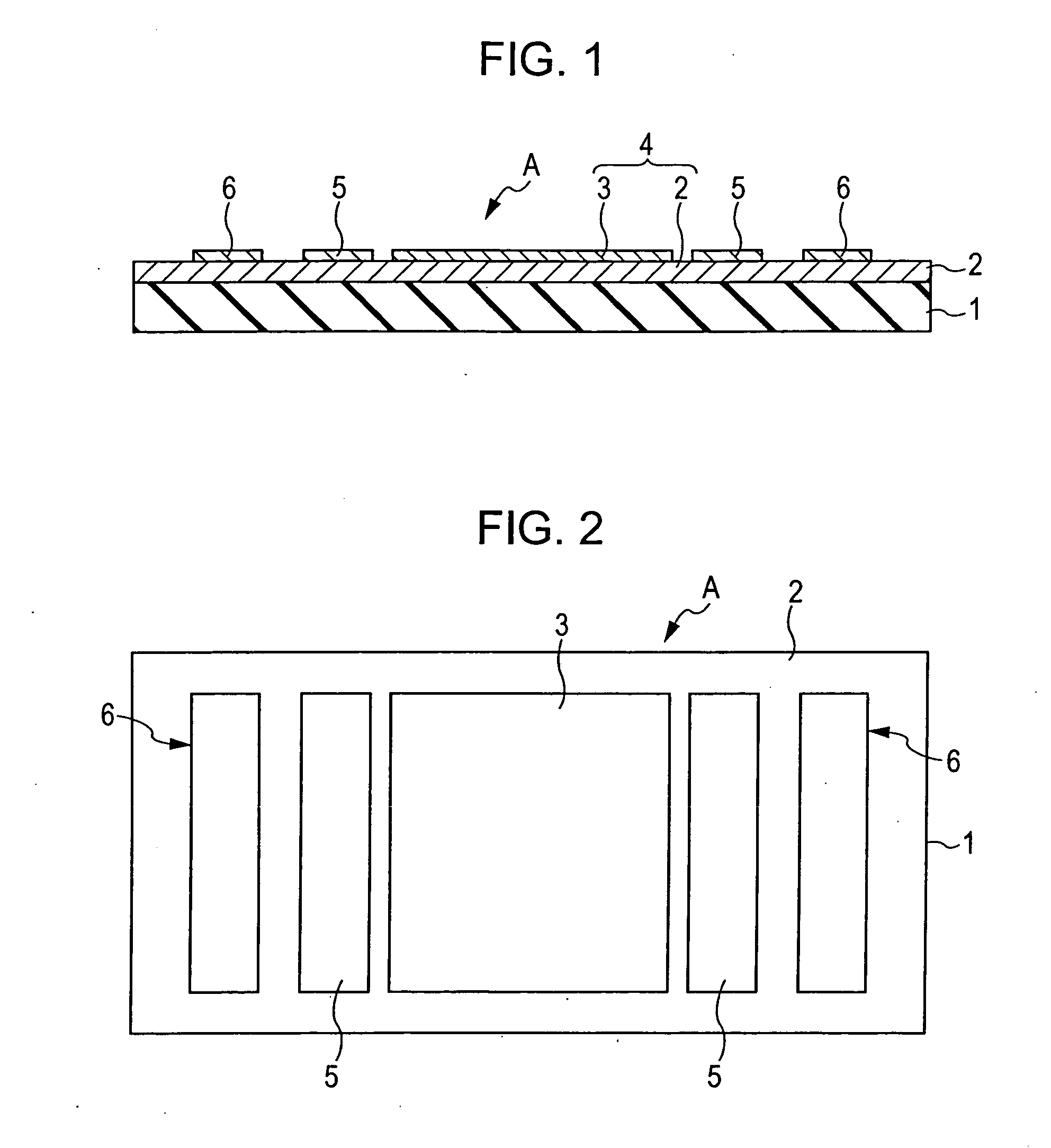
[0051]FIGS. 1 and 2 are views showing the structure of the first embodiment of a hydrogen sensor according to the present invention, and a hydrogen sensor A of this embodiment has the following structure. That is, on the approximately entire upper surface of an insulating substrate (insulating base body) 1, a semiconductor layer (semiconductor) 2 is provided, and at a central portion on the upper surface of this semiconductor layer 2, a hydrogen absorber 3 is formed in which particles are dispersed and arranged in the form of islands. In addition, inside electrodes 5 and 5 and outside electrodes 6 and 6 are provided on the surface of the semiconductor layer 2, the inside ele...
second embodiment
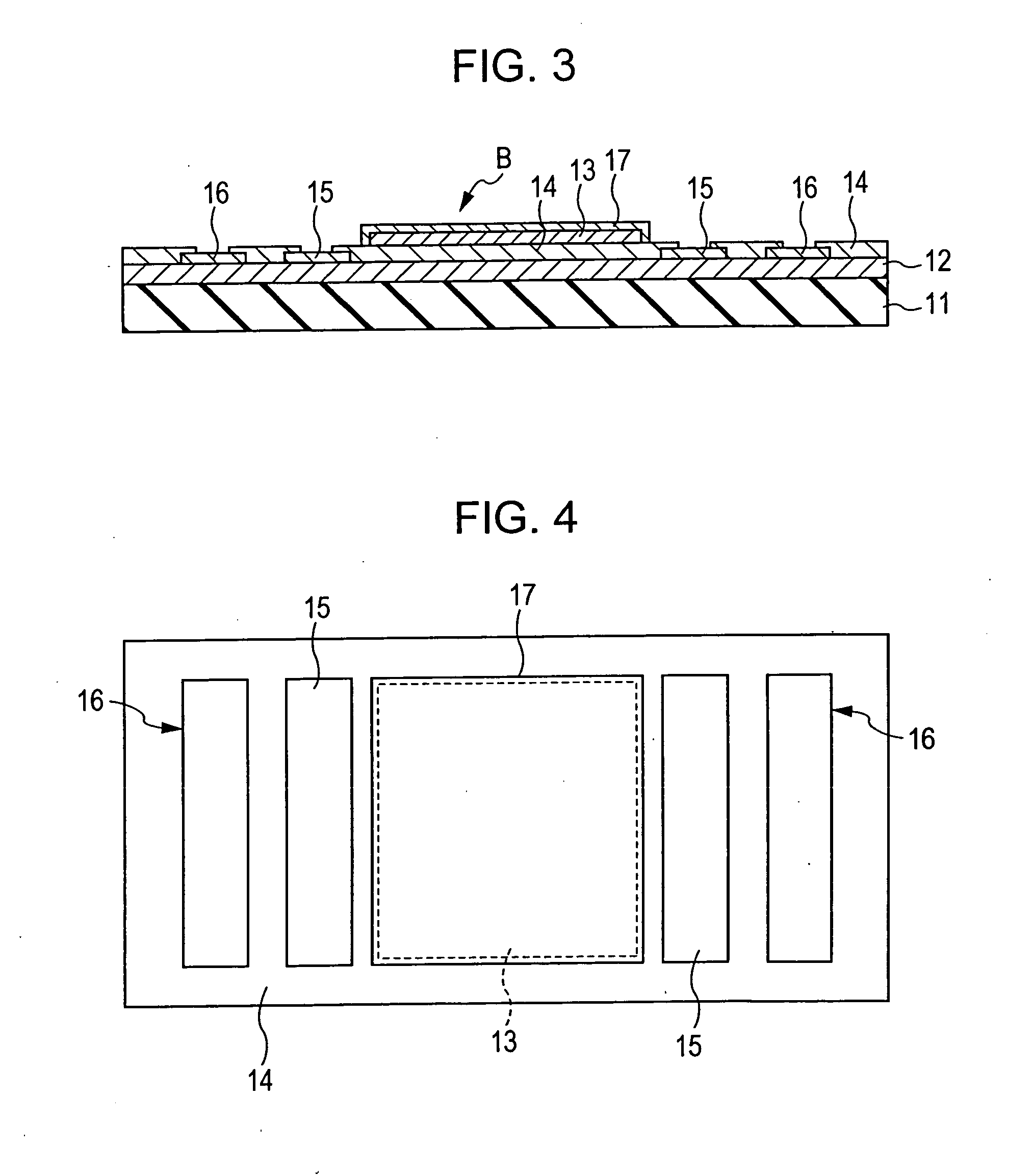
[0063]FIGS. 3 and 4 are views showing the structure of the second embodiment of a hydrogen sensor according to the present invention, and a hydrogen sensor B of this embodiment has the following structure. That is, on the approximately entire upper surface of an insulating substrate 11, a semiconductor layer 12 is provided, and inside electrodes 15 and 15 and outside electrodes 16 and 16 are formed at places located at two sides of a central portion on the upper surface of this semiconductor layer 12, the places being equivalent to those of the case of the hydrogen sensor A of the above first embodiment when viewed in plan. In addition, a thin-film insulating layer 14 is provided so as to cover the peripheral portions of the electrodes 15 and 16 and the other areas, that is, the upper surface of the semiconductor layer 12, and a hydrogen absorber 13 having the structure in which particles are dispersed and arranged in the form of islands is formed so as to be located at the central ...
example 1
[0069] An ITO film (indium tin oxide film) having a thickness of 0.01 μm was formed on a glass substrate 16 mm long and 9 mm wide, and at a central portion of this ITO film, an island-shaped hydrogen absorber film of Pd was formed having a thickness of 12 Å and having a rectangular shape 5 mm long and 7 mm wide. The film of this hydrogen absorber was an insulating member on the glass substrate.
[0070] Subsequently, inside electrodes (inside electrodes each having a laminate structure formed of a Ti layer as an underlayer and a Au layer provided thereon) having a size of 1.2 by 7.5 mm made of a Ti / Au layer were first formed on the ITO film and at two sides of the hydrogen absorber with spaces therefrom, and furthermore, outside electrodes made of a Ti / Au layer were formed outside of the inside electrodes at a distance of 1 mm therefrom.
[0071] The hydrogen sensor having this structure was placed in a measuring chamber, and a repetitive hydrogen gas-detection test was performed in whi...
PUM
 Abstract
Description
Claims
Application Information


