Check patentability & draft patents in minutes with Patsnap Eureka AI!

Method for evaluating semiconductor substrate

a semiconductor substrate and evaluation method technology, applied in semiconductor/solid-state device testing/measurement, data recording, instruments, etc., can solve the problem of insufficient evaluation accuracy of known evaluation methods, and achieve the effect of improving evaluation accuracy more reliably, improving evaluation accuracy, and improving evaluation accuracy

Inactive Publication Date: 2005-11-24
SUMITOMO MITSUBISHI SILICON CORP
View PDF6 Cites 1 Cited by
  • Summary
  • Abstract
  • Description
  • Claims
  • Application Information

AI Technical Summary

Benefits of technology

[0006] Accordingly, an object of the present invention is to provide higher evaluation accuracy.
[0008] The present inventors have studied the cause of variations in evaluation results. The study has found that the variations are due to organic materials adhering to a surface of a semiconductor substrate before a liquid metal electrode is attached to the surface thereof. Such organic materials can be removed by cleaning the semiconductor substrate with SPM before attaching the liquid metal electrode to the surface thereof to achieve higher evaluation accuracy.
[0010] In the evaluation of an SOI substrate, a native oxide film formed on a surface of a surface silicon layer is removed before a liquid metal electrode is attached to the surface of the surface silicon layer. If the substrate is cleaned with SPM after the removal of the native oxide film, the SPM oxidizes the surface of the surface silicon layer to form an oxide film which degrades the evaluation accuracy. The substrate may therefore be cleaned with SPM before the removal of the oxide film to eliminate both the organic materials and the oxide film on the surface of the surface silicon layer.
[0011] The SPM used in the cleaning step may contain 96% sulfuric acid and 29% hydrogen peroxide in a volume ratio of 4:1 to 19:1 to improve the evaluation accuracy more reliably.
[0012] The semiconductor substrate may be cleaned with the SPM by bringing the surface of the semiconductor substrate into contact with the SPM at 100° C. to 160° C. to improve the evaluation accuracy more reliably. In addition, the semiconductor substrate may be cleaned with the SPM by bringing the surface of the semiconductor substrate into contact with the SPM for ten minutes or more to improve the evaluation accuracy more reliably.
[0013] Accordingly, the present invention can provide higher evaluation accuracy.

Problems solved by technology

The study has revealed that known evaluation methods may cause variations in evaluation results for the same semiconductor substrate.
The known evaluation methods therefore have insufficient evaluation accuracy.

Method used


Image

  • Method for evaluating semiconductor substrate
  • Method for evaluating semiconductor substrate
  • Method for evaluating semiconductor substrate

Examples


Embodiment Construction

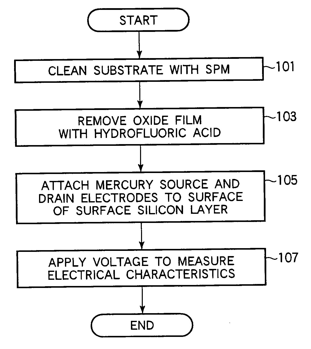
[0027] Methods for evaluating a semiconductor substrate according to embodiments of the present invention will now be described with reference to FIGS. 1 to 11. FIG. 1 is a flow chart of the main steps of a method for evaluating a semiconductor substrate according to an embodiment of the present invention. FIG. 2 is a sectional view showing an example of how electrodes are attached in the evaluation of an SOI substrate. FIGS. 3A, 3B, and 4 schematically show that parasitic capacitance occurs when organic materials adhere to a surface of the SOI substrate to be evaluated. FIG. 5A is a graph showing measurements by gas chromatography-mass spectrometry in the case where the SOI substrate was not cleaned with SPM. FIG. 5B is a graph showing measurements by gas chromatography-mass spectrometry in the case where the SOI substrate was cleaned with the SPM to remove the organic materials.

[0028]FIG. 6 is a graph showing Ids-Vgs curves in the cases where the SOI substrate was cleaned and not...


PUM

PropertyMeasurementUnit
temperatureaaaaaaaaaa
diameteraaaaaaaaaa
temperaturesaaaaaaaaaa

Abstract

A method for evaluating a semiconductor substrate includes the steps of cleaning the semiconductor substrate with SPM, attaching a liquid metal electrode to a surface of the semiconductor substrate, and applying a voltage to the semiconductor substrate.

Description

BACKGROUND OF THE INVENTION [0001] 1. Field of the Invention [0002] The present invention relates to methods for evaluating a semiconductor substrate by attaching a liquid metal electrode to a surface thereof. [0003] 2. Description of the Related Art [0004] In recent years, the demand for higher reliability on semiconductor layers, such as silicon layers, and insulating films, such as silicon oxide films, has been growing with increasing packing density of, for example, LSIs having a metal-insulator-semiconductor (MIS) structure. Under such circumstances, the electrical characteristics of semiconductor layers and insulating films included in semiconductor substrates are evaluated by evaluation methods in which an electrode made of a liquid metal such as mercury is attached to a surface of a semiconductor substrate to achieve higher evaluation accuracy. Such methods have been proposed in, for example, the following documents: U.S. Pat. No. 6,429,145 (Paragraphs 2 to 6, FIG. 2); U.S. ...

Claims


Application Information

Patent Timeline
Patent Type & Authority Applications(United States)
IPC IPC(8): H01L21/66G11B9/00H01L21/304H01L21/308H01L27/12
CPCH01L22/14H01L2924/0002H01L2924/00
Inventor YAMAZAKI, TORU
Owner SUMITOMO MITSUBISHI SILICON CORP
Features
  • R&D
  • Intellectual Property
  • Life Sciences
  • Materials
  • Tech Scout
  • Unparalleled Data Quality
  • Higher Quality Content
  • 60% Fewer Hallucinations
Learn More