Semiconductor device

a technology of semiconductors and devices, applied in the direction of semiconductor devices, electrical equipment, transistors, etc., can solve the problem of limiting the acceleration of switching speeds

Active Publication Date: 2005-12-01
KK TOSHIBA
View PDF14 Cites 77 Cited by
  • Summary
  • Abstract
  • Description
  • Claims
  • Application Information

AI Technical Summary

Benefits of technology

[0016] A semiconductor device according to further embodiment of the invention comprises a first base layer of a first conductivity type; a plurality of second base layers of a second conductivity type, provided on a part of a first surface of the first base layer; trenches formed entirely between the second base layers adjacent to each other so as to be wider than the second base layers and to be deeper than the second base layers; an emitter layer formed along the trench on a surface of the second base layer; a collector layer of the second conductivity type, provided on a second surface of the first base layer opposite to the first surface; an insulating film formed on an inner wall of the trench; a gate electrode formed within the trench, the gate electrode being isolated from the second base layers and the emitter layer by the insulating film; and a bottom semiconductor layer of the first conductivity type, provided on a bottom of the trench, the bottom semiconductor layer being electrically isolated from the emitter layer and the second base layers, and being higher in impurity concentration than the first base layer.
[0017] A semiconductor device according to further embodiment of the invention comprises a first base layer of a first conductivity type; a plurality of second base layers of a second conductivity type, provided on a part of a first surface of the first base layer; trenches formed on each side of the second base layers, and formed to be deeper than the second base layers; an emitter layer formed along the trench on a surface of the second base layers; a collector layer of the second conductivity type, provided on a second surface of the first base layer opposite to the first surface; an insulating film formed on an inner wall of the trench; a gate electrode formed within the trench, and isolated from the second base layers and the emitter layer by an insulating film; and a space section including a semiconductor layer of the first conductivity type, the semiconductor layer being provided between the second base layers adjacent to each other and being electrically isolated from the emitter layer and the second base layers, the semiconductor layer being higher in impurity concentration than the first base layer.

Problems solved by technology

The IGBT and the IEGT is large in capacity COX generated by a gate oxide film, so that there is a limit to acceleration of a switching speed.

Method used


Image

  • Semiconductor device
  • Semiconductor device
  • Semiconductor device

Examples


fifth embodiment

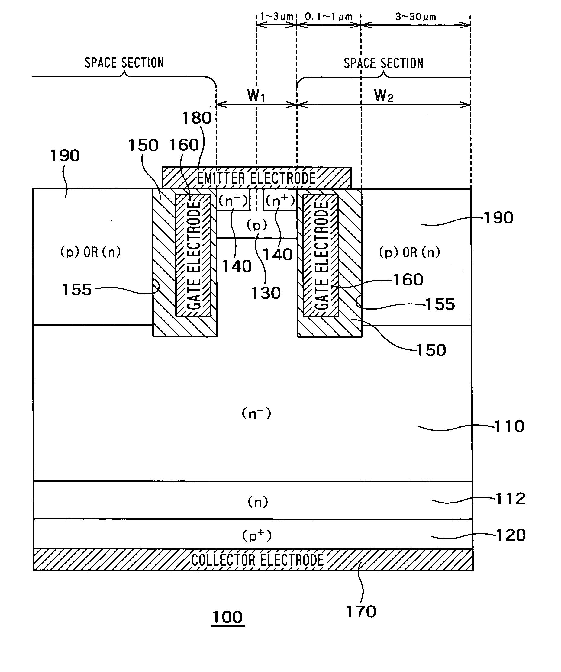
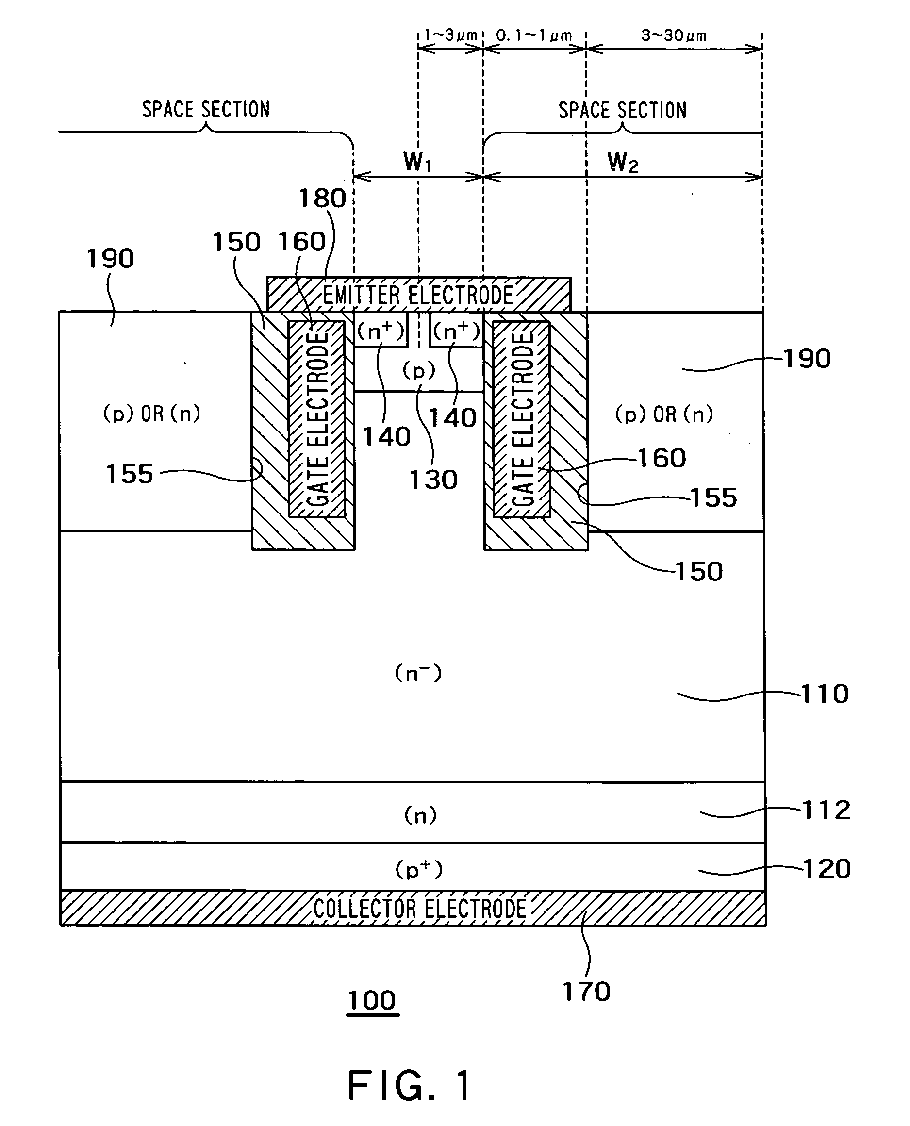
[0065]FIG. 6 is a cross-sectional view of a MOS semiconductor device 500 according to a fifth embodiment of the present invention. The fifth embodiment differs from the first to the fourth embodiments in that the semiconductor layer 190 and the bottom semiconductor layer 200 are not provided and in that the insulating film 150 and the gate electrode 160 are formed in each entire space section. According to the fifth embodiment, the insulating film 150 and the gate electrode 160 function as the space section into which no holes flow. Therefore, the width W2 of the trench 155 (width of the insulating film 150 or the gate electrode 160) corresponds to that of the space section.

[0066] The fifth embodiment exhibits the same advantages as those of the first embodiment. Furthermore, since it is unnecessary to form the semiconductor layer 190 and the bottom semiconductor layer 200, the semiconductor device 500 of the fifth embodiment can be manufactured easily, as compared with the first t...

sixth embodiment

[0067]FIG. 7 is a cross-sectional view of a MOS semiconductor device 600 according to a sixth embodiment of the present invention. The sixth embodiment differs from the fifth embodiment by providing the bottom semiconductor layer 200 on the bottom of each trench 155. The bottom semiconductor layer 200 exhibits the same advantages as those of the bottom semiconductor layer 200 according to the third embodiment. Therefore, a switching speed of the semiconductor device 600 according to the sixth embodiment can be further accelerated, as compared with the fifth embodiment. In addition, injection efficiency can be further improved, as compared with the fifth embodiment.

[0068] In the sixth embodiment, the bottom semiconductor layer 200 may be formed of an n-type semiconductor higher in impurity concentration than the first base layer 110. By so forming, the IE effect can be improved.

seventh embodiment

[0069]FIG. 8 is a cross-sectional view of a MOS semiconductor device 700 according to a seventh embodiment of the present invention. According to the seventh embodiment, the gate electrode 160 is provided within each trench 155 through the insulating film 150, and the insulating film 150 is further filled into inside of the gate electrode 160. The other constituent elements of the semiconductor device 700 according to the seventh embodiment may be same as those of the semiconductor device 600 according to the sixth embodiment.

[0070] In the seventh embodiment, an interior of the trench 155 is manufactured as follows. The insulating film 150 and a gate electrode material are sequentially deposited on an inner wall of the trench 155. At this time, the gate electrode material is deposited by a film thickness sufficient to cover sidewalls of the trench 155 without entirely filling the gate electrode material into the trench 155. Further, the insulating film 150 is deposited on this gate...


PUM


Abstract

A semiconductor device comprises a first base layer of a first conductivity type; a plurality of second base layers of a second conductivity type, provided on a part of a first surface of the first base layer; trenches formed on each side of the second base layers, and formed to be deeper than the second base layers; an emitter layer formed along the trench on a surface of the second base layers; a collector layer of the second conductivity type, provided on a second surface of the first base layer opposite to the first surface; an insulating film formed on an inner wall of the trench, the insulating film being thicker on a bottom of the trench than on a side surface of the trench; a gate electrode formed within the trench, and isolated from the second base layers and the emitter layer by the insulating film; and a space section provided between the second base layers adjacent to each other, the space section being deeper than the second base layers and being electrically isolated from the emitter layer and the second base layers.

Description

CROSS-REFERENCE TO RELATED APPLICATION [0001] This application is based upon and claims the benefit of priority from the prior Japanese Patent Applications No. 2004-159468, filed on May 28, 2004, the entire contents of which are incorporated herein by reference. BACKGROUND OF THE INVENTION [0002] 1. Field of the Invention [0003] The present invention relates to a semiconductor device. [0004] 2. Background Art [0005] In recent years, an IGBT (Insulated Gate Bipolar Transistor) is widely used as a power semiconductor device having a breakdown voltage of 600 V or more. Since the IGBT is normally used as a switch, it is desired to be low in ON resistance and high in switching speed. [0006] The widely used IGBT having a trench structure includes a p-type base and an n-type base vertically adjacent to each other, an n-type emitter provided on a surface of the p-type base, and a p-type collector provided on a rear surface of the n-type base. If a positive bias is applied to a gate electrod...

Claims


Application Information

Patent Timeline
Patent Type & Authority Applications(United States)
IPC IPC(8): H01L29/78H01L27/082H01L29/08H01L29/10H01L29/423H01L29/739
CPCH01L29/0834H01L29/7397H01L29/1095
Inventor OGURA, TSUNEOYAMAGUCHI, MASAKAZUINOUE, TOMOKININOMIYA, HIDEAKISUGIYAMA, KOICHI
Owner KK TOSHIBA
Why Eureka
Try Eureka