Automatic biasing of a power device for linear operation
Inactive Publication Date: 2005-12-01
AVAGO TECH WIRELESS IP SINGAPORE PTE
View PDF8 Cites 3 Cited by
Summary
Abstract
Description
Claims
Application Information
AI Technical Summary
This helps you quickly interpret patents by identifying the three key elements:
Problems solved by technology
Method used
Benefits of technology
Benefits of technology
[0008] In accordance with the principles of the present invention, a system for biasing an electronic circuit containing a non-linear device is provided. An electronic circuit containing a non-linear device produces an output analog signal from an input analog signal. A sensing circuit coupled to the electronic circuit produces a first signal proportional to a first transconductance value of the non-linear device,
Problems solved by technology
However, as is appreciated by the present inventors, we do not live in an ideal world.
As such, conventional devices nevertheless have some amount of degradation due to process and / or temperature variations.
Thus, any sensitivity of the linearity of a power device such as a power transistor to temperature directly translates into a potential reduction in the product yield.
Method used
Image
Click on the blue label to locate the original text in one second.
Reading with bidirectional positioning of images and text.
Examples
first embodiment
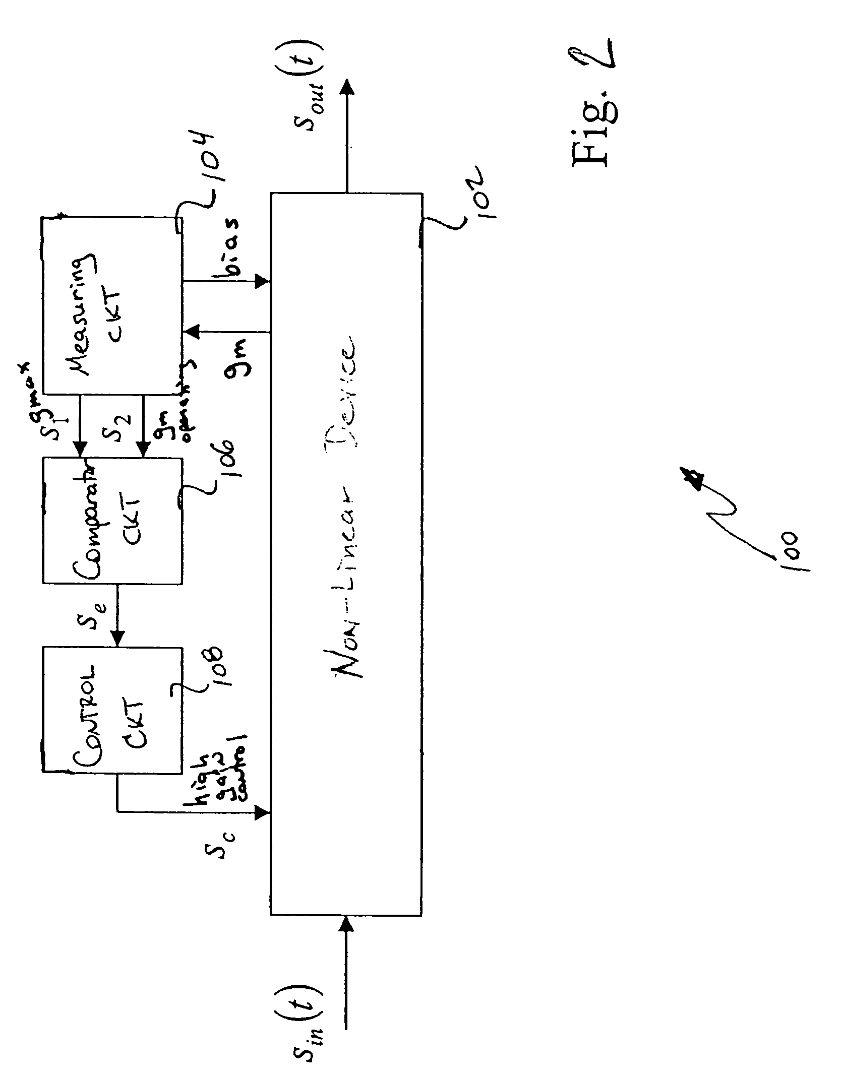
[0033]FIG. 2 shows the present invention wherein a measuring circuit measures the transconductance of the non-linear device at two distinct operating points, in accordance with the principles of the present invention. The circuit of FIG. 2 provides true feedback in that the gm that needs to be constrained is measured directly.
[0035] The electronic circuit 102 is any device that produces an analog output signal from an analog input signal. The electronic circuit 102 contains a non-linear device (e.g., a Class AB amplifier) that can be characterized using a non-constant transconductance (gm) to voltage relationship. The electronic circuit 102 includes a terminal that changes the operating point of the non-linear device and alters device transconductance.
[0036] The measuring circuit 104...
second embodiment
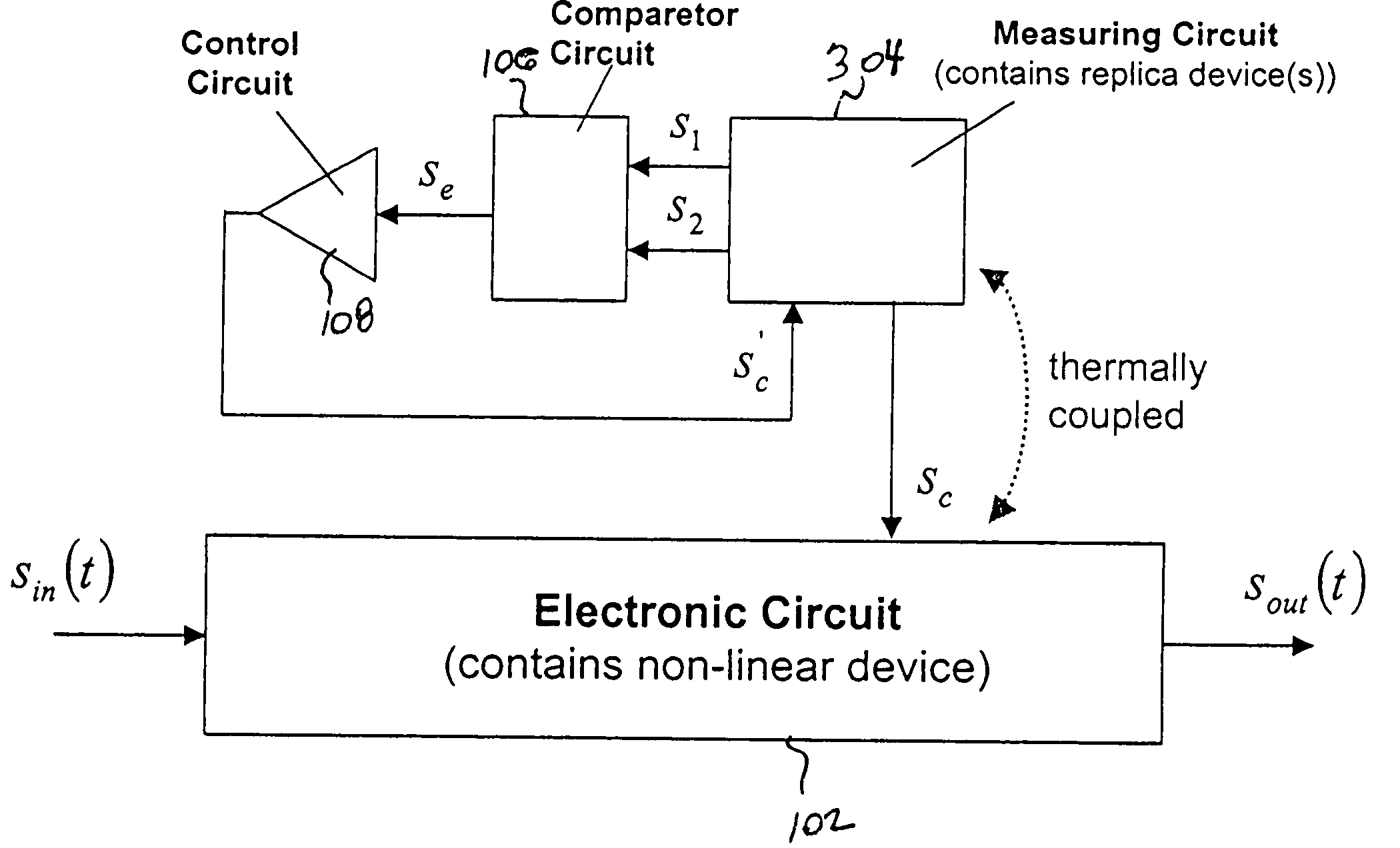
[0043]FIG. 3 shows the present invention wherein a measuring circuit including replica device(s) measures the transconductance of the non-linear device at two distinct operating points, in accordance with the principles of the present invention.
[0044] In particular, as shown in FIG. 3, a master-slave topology is formed. Importantly, the feedback loop does not include the electronic circuit whose transconductance gm will be constrained. Rather, the loop is built around a replica device(s) and the desired transconductance (gm) constraint is achieved indirectly by similarity between the replica devices in the measuring circuit 304, and the non-linear device in the electronic circuit 102.
[0045] The circuit of FIG. 3 is easier to implement because no measurements are taken directly upon the non-linear device, so the signal processing in the electronic circuit 102 may continue uninterrupted.
[0046] Equations governing the operation of the system shown in FIG. 3 are as follows. Equations ...
third embodiment
[0050]FIG. 4 shows the present invention wherein two separate measuring circuits each including replica device(s) measure the transconductance of the non-linear device at two distinct operating points, in accordance with the principles of the present invention.
[0051] In particular, as shown in FIG. 4, a master-slave topology is implemented similar to that of FIG. 3, but using two separate measuring circuits 404, 405, each containing its own replica device. The circuit of FIG. 4 is easy to implement because no measurements are made upon the non-linear device in the electronic circuit 102. The signals S1, S2 output respectively from the two measuring circuits 404, 405, are derived by measuring two separate replica devices. The system of FIG. 4 assumes similarity between the non-linear device of the electronic circuit 102 and the replica devices used in the first measuring circuit as well as the replicas used in the second measuring circuit.
PUM
Abstract
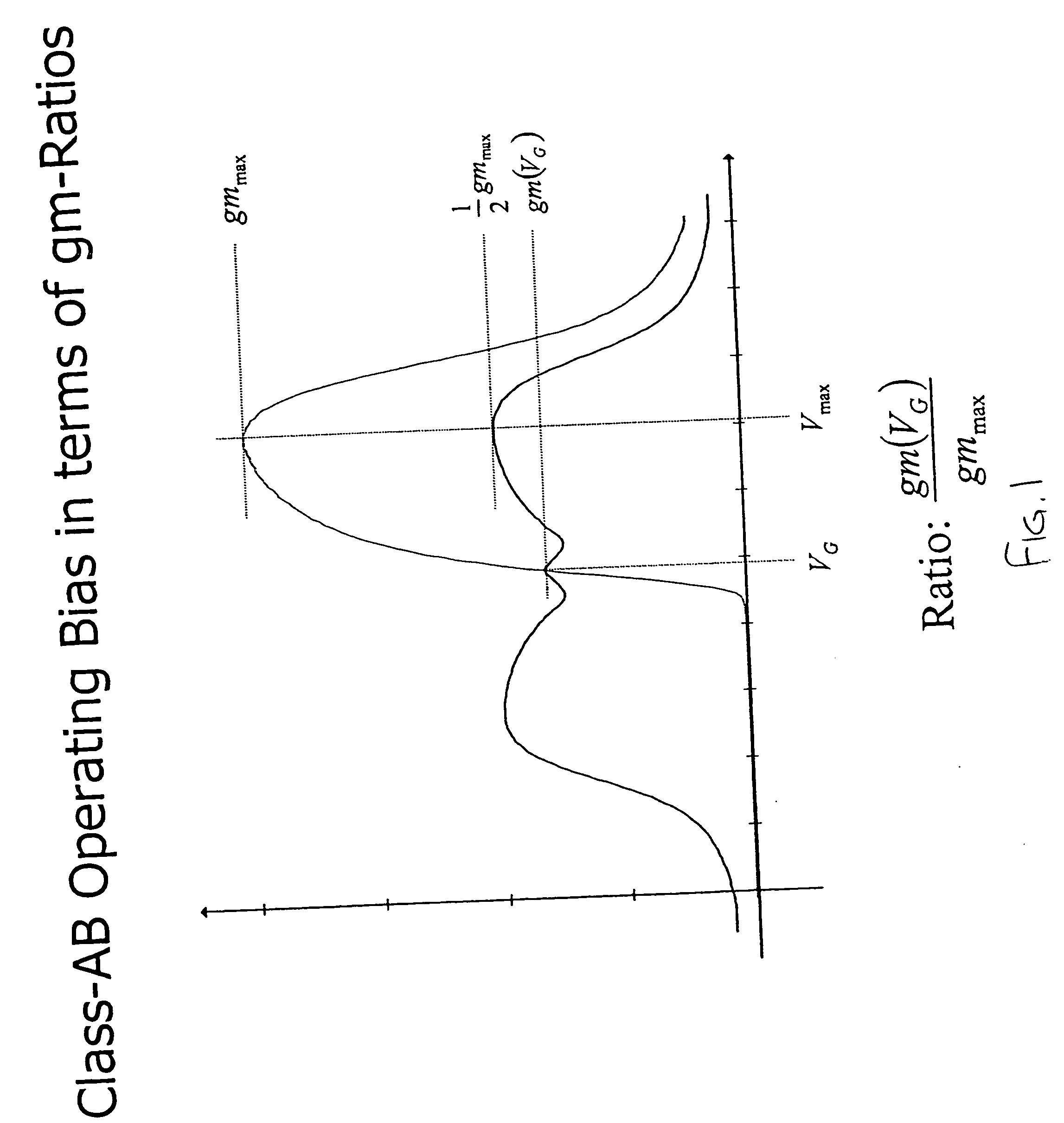
A power device(s) is biased and operates in Class-AB. A purpose of the disclosed embodiments is to minimize crossoverdistortion over a broad range of operating conditions, not only for a nominal case. The bias current of a power transistor is automatically adjusted in response to process and temperature variations. Preferably, the adjustment is performed using an error-feedback arrangement. An exemplary ‘rule’ for bias adjustment involves satisfying a proportionality relationship between the small-signal device transconductance at the operating point, and a maximum device transconductance. The disclosed adaptive bias scheme utilizes a dual replica master-slave control architecture. A self-adapting circuit is provided to change the bias current (or voltage) so that the value is always the optimum value, irrespective of operating temperature and / or process variations. Self-biasing is introduced wherein no manual adjustment is necessary, thereby saving production or lab time. Amplifier robustness to process and temperature variations is improved, increasing yield.
Description
BACKGROUND OF THE INVENTION [0001] 1. Field of the Invention [0002] This invention relates to power devices, modules and amplifiers. More particularly, it relates to biasing of a power transistor. [0003] 2. Background of Related Art [0004] As is known, a very specific bias is required to ensure the linearity of Class-AB power amplifiers. However, the value of the required ‘optimum’ bias current varies somewhat with process and temperature. [0005] To accommodate this variation, conventional devices provide a fixed bias (usually current) such that under nominal conditions, the best linearity is achieved. Ideally such conventional device would be maintained in an environmental condition to maintain it as close as possible to the nominal conditions (e.g., at a given temperature). However, as is appreciated by the present inventors, we do not live in an ideal world. As such, conventional devices nevertheless have some amount of degradation due to process and / or temperature variations. [0...
Claims
Application Information
Patent Timeline
Application Date:The date an application was filed.
Publication Date:The date a patent or application was officially published.
First Publication Date:The earliest publication date of a patent with the same application number.
Issue Date:Publication date of the patent grant document.
PCT Entry Date:The Entry date of PCT National Phase.
Estimated Expiry Date:The statutory expiry date of a patent right according to the Patent Law, and it is the longest term of protection that the patent right can achieve without the termination of the patent right due to other reasons(Term extension factor has been taken into account ).
Invalid Date:Actual expiry date is based on effective date or publication date of legal transaction data of invalid patent.

