Solder paste lateral flow and redistribution system and methods of same

Inactive Publication Date: 2005-12-08
SPEEDLINE TECH
View PDF11 Cites 16 Cited by
  • Summary
  • Abstract
  • Description
  • Claims
  • Application Information

AI Technical Summary

Benefits of technology

[0011] Various aspects of the invention may provide one or more of the following advantages. Solder pastes, adhesives or other materials can be used effectively in stencil printing electronic substrates, such as circuit board assemblies, by minimizing or eliminating material waste or runoff produced during stenciling processes. For instance, solder paste waste or runoff, e.g., solder paste migrating toward edges of a stencil and other hard-to-reach areas of a stencil during a stenciling process, can be remixed with bulk solder paste used in the process and / or can be redistributed across the stencil to help to eliminate or reduce the amount of solder paste waste. Remixing excess solder paste during a stencil process helps to maintain a desired theology of solder paste employed and to thereby enable excess or runoff solder paste to be reused during stenciling. Redistributing excess or runoff solder paste during a stencil process helps to reduce or to eliminate local compaction of excess or runoff solder paste in areas of a stencil defining a high density of fine apertures. Remixing and redistributing excess or runoff solder paste enables all or substantially all of the apertures defined in a surface of a stencil receive solder paste to deposit there through to a surface of an electronic substrate.

Problems solved by technology

As the wiping blade typically cannot reach the stencil edges, solder paste runoff tends to go to waste unless an operator regularly mixes the runoff disposed along the stencil edges, or other hard-to reach-areas of the stencil, with bulk paste used in the stenciling process or with material remaining on the stencil.
Without remixing or redistributing solder paste runoff, the theology of the paste changes rapidly and, as a result, cannot be remixed or used.
In addition, during the printing process, solder paste tends to compact along regions of the stencil having a high density of fine apertures.
Without an ability to remix or redistribute solder paste disposed along such regions, current squeegee devices are incapable of delaying or preventing local solder paste compaction on stencil surfaces.

Method used


Image

  • Solder paste lateral flow and redistribution system and methods of same
  • Solder paste lateral flow and redistribution system and methods of same
  • Solder paste lateral flow and redistribution system and methods of same

Examples


Embodiment Construction

[0019] Embodiments of the present invention are described below with reference to screen printers or stencil printers that print solder paste, adhesive or other materials onto circuit boards. As understood by those of ordinary skill in the art, embodiments of the present invention can be used with electronic substrates other than circuit boards and with machines other than screen printers.

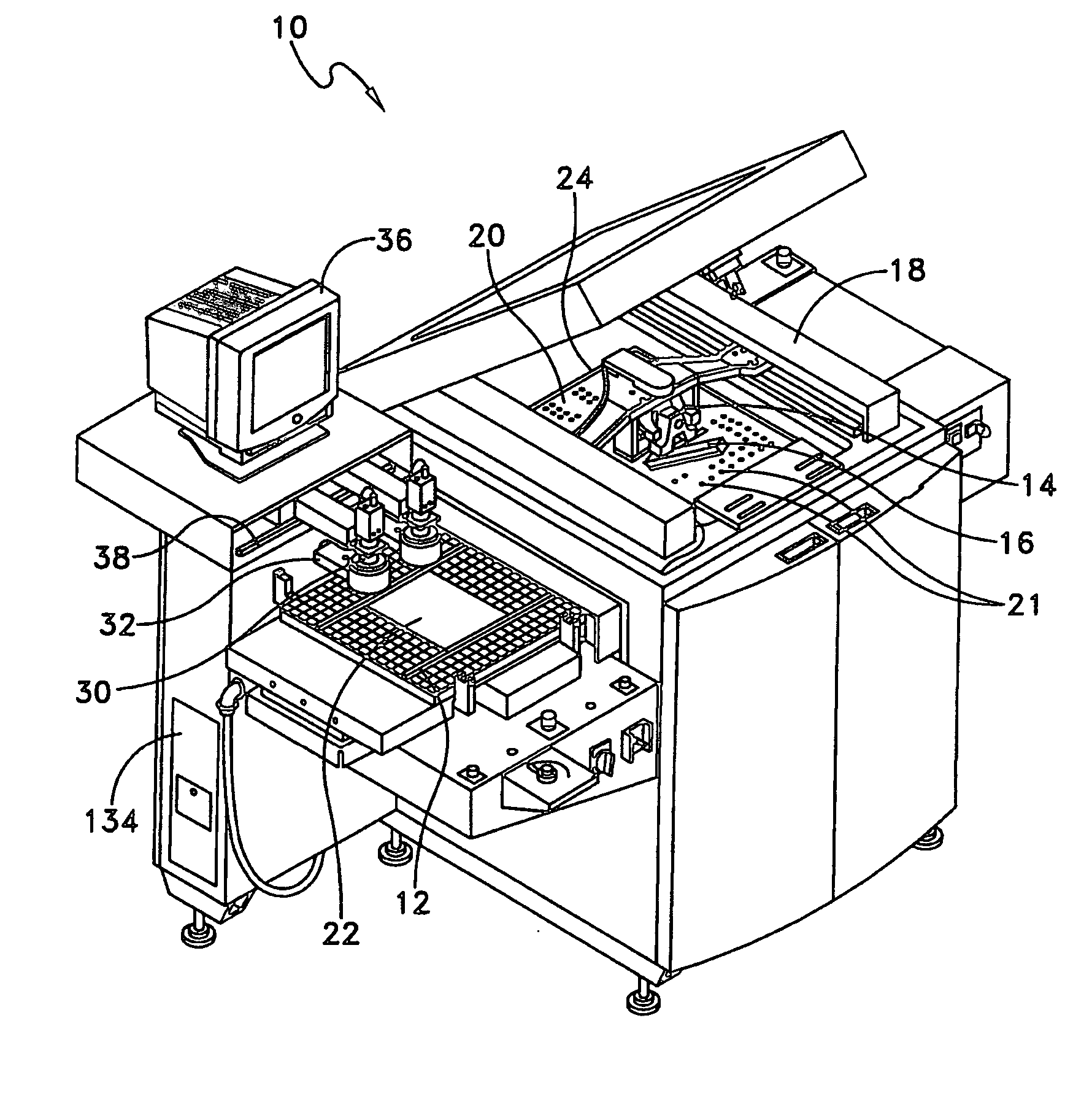
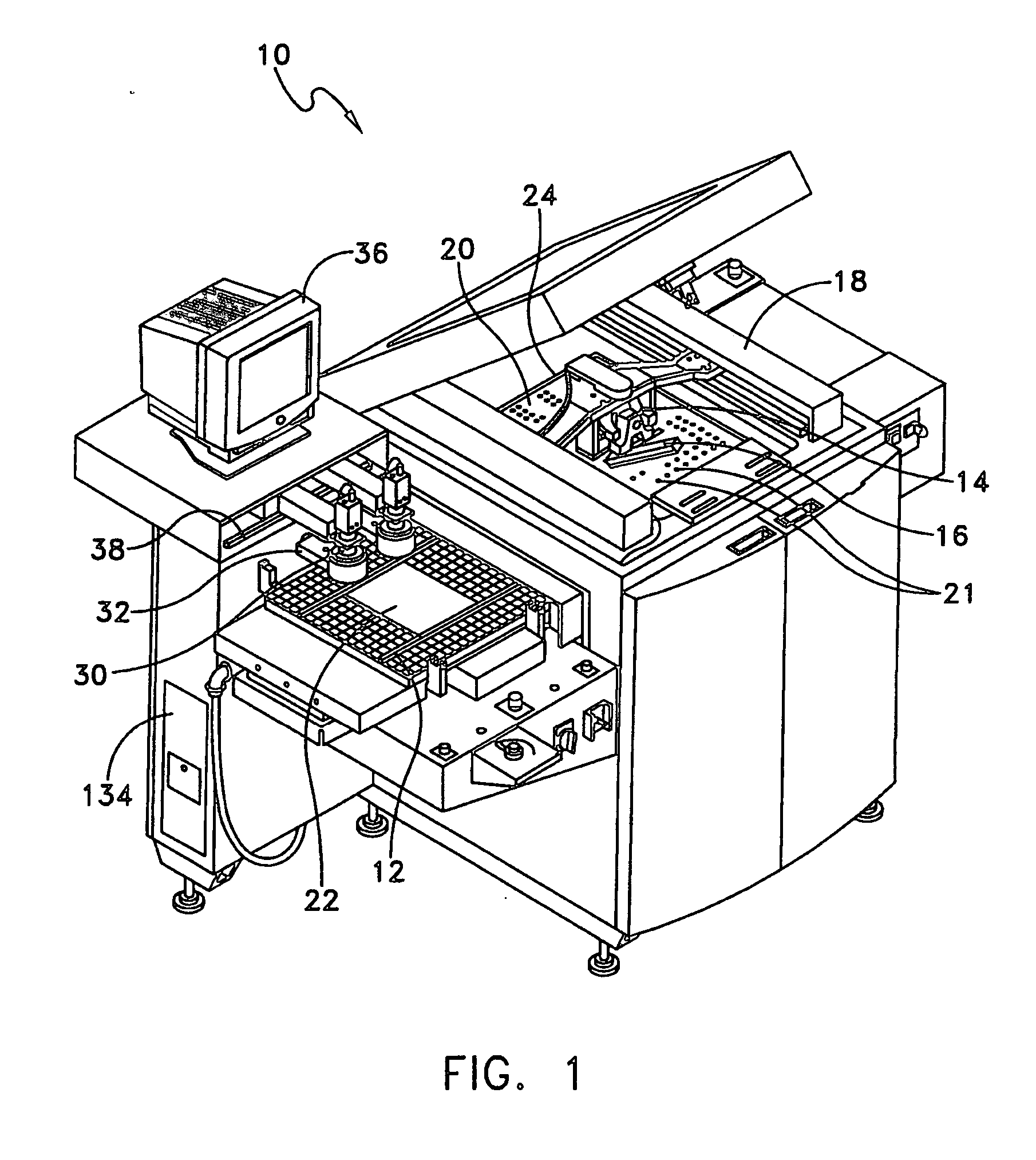
[0020] Referring to FIG. 1, a printer 10 in accordance with one embodiment of the invention that applies solder pastes, adhesives or other materials to substrates, such as circuit boards, is shown. The printer is an improvement over the screen printer described in U.S. Pat. No. 5,794,329, U.S. Pat. No. 6,324,973 and U.S. patent application Ser. No. 10 / 236,108, each of which is hereby incorporated by reference.

[0021] As shown in FIG. 1, the printer 10 includes a tractor feed mechanism 12 coupled to a printer frame to support and to transfer a substrate, e.g., a circuit board 22, a material dispens...


PUM


Abstract

An apparatus and methods for depositing material on a surface of an electronic substrate are provided and include a squeegee device or system for distributing material to be deposited on the electronic substrate. The squeegee device or system can include a first wiping blade and a second wiping blade spaced from and parallel to the first wiping blade. The first wiping blade and the second wiping blade are disposed at an angle relative to a vertical axis, the vertical axis being perpendicular to a surface of an electronic substrate, such that when the first and the second wiping blades contact a surface of a stencil to deposit or print the material onto the electronic substrate, the first and the second wiping blades contact the stencil surface at a rake angle relative to a direction in which the squeegee device traverses the stencil surface. The rake angle of the first and the second wiping blades enables the squeegee device to traverse the stencil surface at an angle, which causes the material deposited in front of either wiping blade to flow laterally in one direction toward an end of the wiping blade during a print stroke. In addition, the first wiping blade is offset relative to the second wiping blade such that as the material laterally flows in front of one of the wiping blades and runs off the end of the wiping blade during a print stroke, the other wiping blade is positioned to retrieve the material runoff and to thereby remix or redistribute the material runoff across the stencil surface during a print stroke in an opposite direction.

Description

FIELD OF THE INVENTION [0001] The invention relates to apparatus and methods for screen printing, and more specifically to apparatus and methods for the screen printing of electronic substrates such as circuit board assemblies. BACKGROUND OF THE INVENTION [0002] Manufacturing circuit boards involves a number of processes, one of which is the screen or stencil printing of solder paste and adhesives onto printed circuit boards in order to deposit electronic components onto the boards. A stencil having an aperture or, more typically, a plurality of apertures defines a pattern that corresponds to a pattern of pads or, usually conductive, surface areas disposed on or defined in a surface of a circuit board to which electronic components are mounted. The stencil is used to apply solder paste, adhesive or other materials to the pads or conductive surface areas such that surface mount electronic components can be disposed on and thereafter adhered to the surface of the circuit board. The st...

Claims


Application Information

Patent Timeline
IPC IPC(8): B41F15/08B41F15/44B41F15/46H05K3/12
CPCB41F15/0818H05K2203/0139H05K3/1233B41F15/44
Inventor PHAM-VAN-DIEP, GERALD C.PRINCE, DAVID P.
Owner SPEEDLINE TECH
Why Eureka
Try Eureka