Replacement gate process for making a semiconductor device that includes a metal gate electrode

a metal gate electrode and replacement gate technology, applied in the direction of semiconductor devices, basic electric elements, electrical equipment, etc., can solve the problems of adversely affecting the subsequent polysilicon removal steps

Inactive Publication Date: 2005-12-08
INTEL CORP
View PDF24 Cites 75 Cited by
  • Summary
  • Abstract
  • Description
  • Claims
  • Application Information

AI Technical Summary

Problems solved by technology

Silicide may form at those exposed corners, when the source and drain regions are silicided, which may adversely impact the subsequent polysilicon removal steps.

Method used


Image

  • Replacement gate process for making a semiconductor device that includes a metal gate electrode
  • Replacement gate process for making a semiconductor device that includes a metal gate electrode
  • Replacement gate process for making a semiconductor device that includes a metal gate electrode

Examples


Embodiment Construction

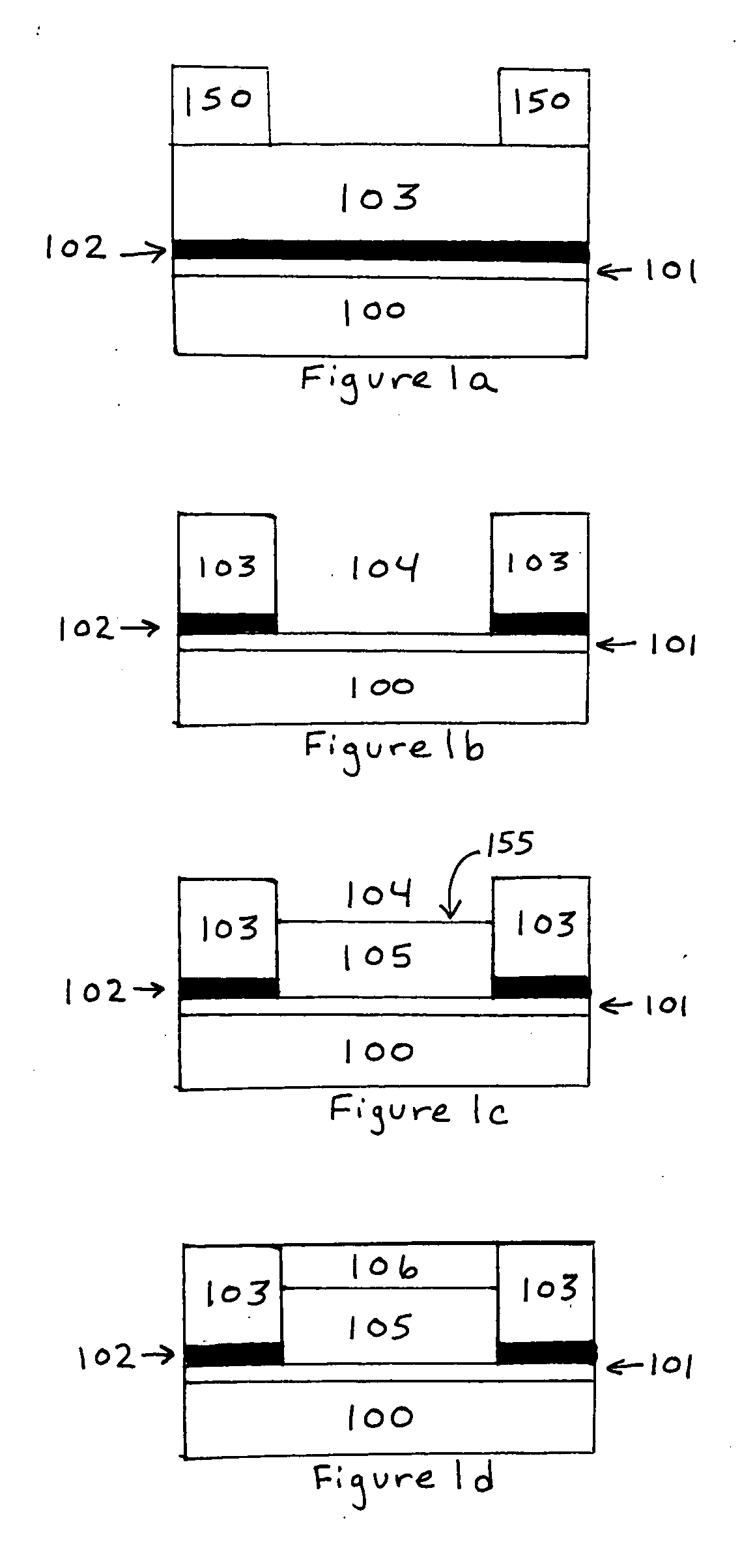
[0008] A method for making a semiconductor device is described. That method comprises forming a sacrificial layer on a substrate, and forming a trench within the sacrificial layer. After forming a dummy gate electrode within the trench, a hard mask is formed on the dummy gate electrode and within the trench. In the following description, a number of details are set forth to provide a thorough understanding of the present invention. It will be apparent to those skilled in the art, however, that the invention may be practiced in many ways other than those expressly described here. The invention is thus not limited by the specific details disclosed below.

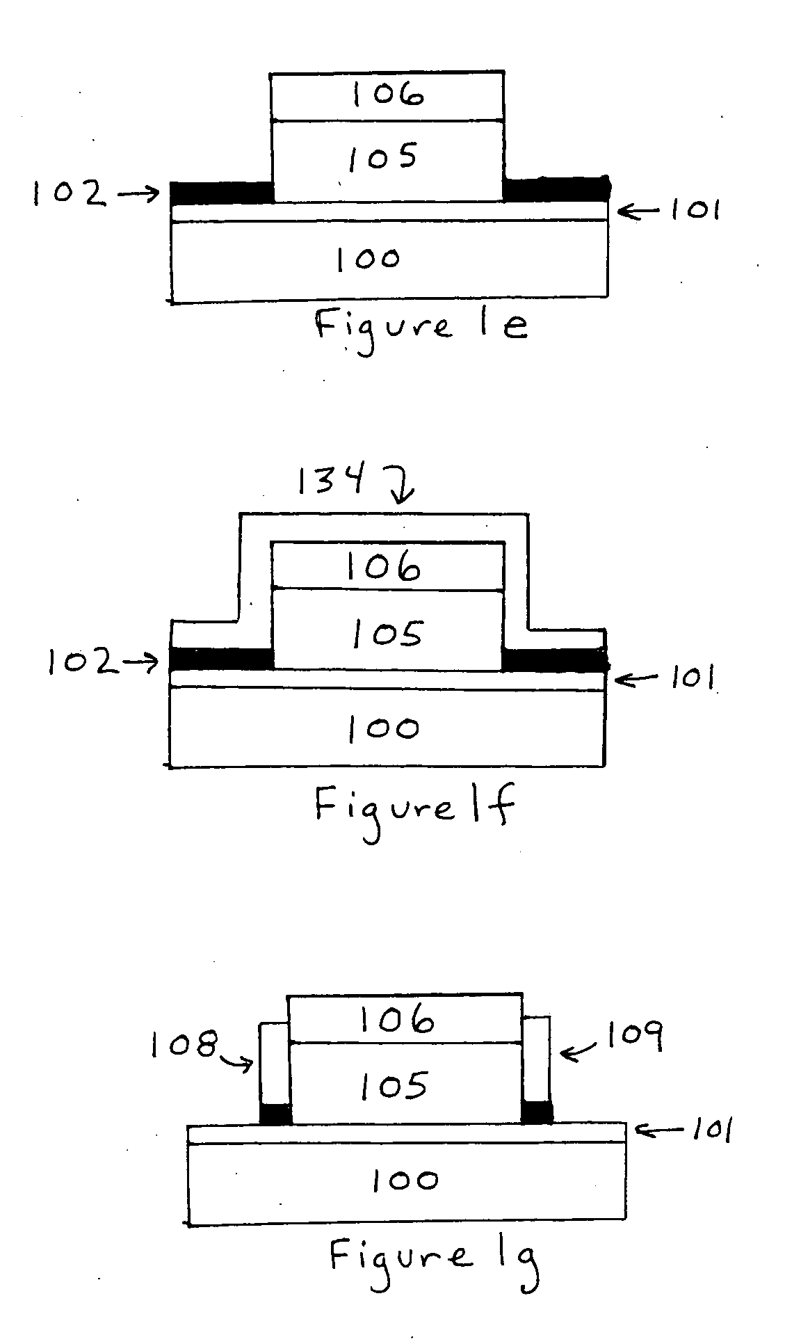
[0009]FIGS. 1a-1g illustrate structures that may be formed, when carrying out an embodiment of the method of the present invention. Initially, dielectric layer 101 is formed on substrate 100, etch stop layer 102 is formed on dielectric layer 101, and sacrificial layer 103 is formed on etch stop layer 102. Masking layer 150 is then dep...


PUM


Abstract

A method for making a semiconductor device is described. That method comprises forming a sacrificial layer on a substrate, and forming a trench within the sacrificial layer. After forming a dummy gate electrode within the trench, a hard mask is formed on the dummy gate electrode and within the trench.

Description

FIELD OF THE INVENTION [0001] The present invention relates to methods for making semiconductor devices, in particular, semiconductor devices with metal gate electrodes. BACKGROUND OF THE INVENTION [0002] When making a CMOS device that includes metal gate electrodes, a replacement gate process may be used to form gate electrodes from different metals. In that process, a first polysilicon layer, bracketed by a pair of spacers, is removed to create a trench between the spacers. The trench is filled with a first metal. A second polysilicon layer is then removed, and replaced with a second metal that differs from the first metal. [0003] In such a process, it may be necessary to form a hard mask on the polysilicon layers to minimize silicide formation, when the transistors' source and drain regions are covered with a silicide. Although such a hard mask may protect the upper surface of the polysilicon layers, the upper corners of those layers may be exposed, when the spacers are formed. S...

Claims


Application Information

Patent Timeline
Patent Type & Authority Applications(United States)
IPC IPC(8): H01L21/28H01L21/3205H01L21/336H01L21/338H01L21/8234H01L21/8238H01L29/49H01L29/51H01L29/78
CPCH01L21/28185H01L21/28194H01L21/823842H01L21/823857H01L29/495H01L29/4966H01L29/513H01L29/517H01L29/66545H01L29/66583H01L29/7833
Inventor SHAH, UDAYDOCZY, MARK L.BRASK, JUSTIN K.KAVALIEROS, JACKMETZ, MATTHEW V.CHAU, ROBERT S.BARNS, CHRIS E.
Owner INTEL CORP
Why Eureka
Try Eureka