

Random access memory
a random access and memory technology, applied in the direction of capacitors, semiconductor devices, electrical devices, etc., can solve the problems of chip itself being defective, unable to be used, and unable to store information, so as to improve the refresh rate of dynamic access memory devices
- Summary
- Abstract
- Description
- Claims
- Application Information
AI Technical Summary
Benefits of technology
Problems solved by technology
Method used
Image

Examples
Embodiment Construction
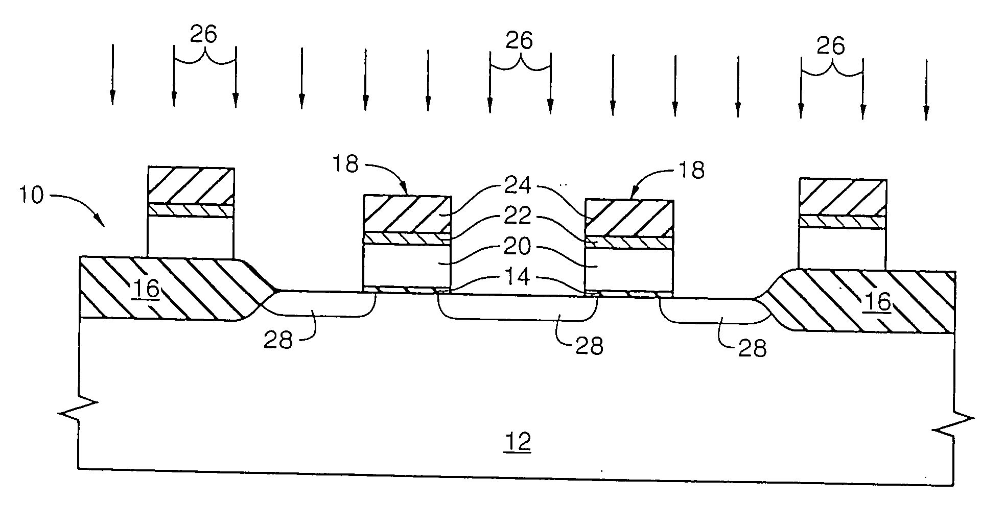
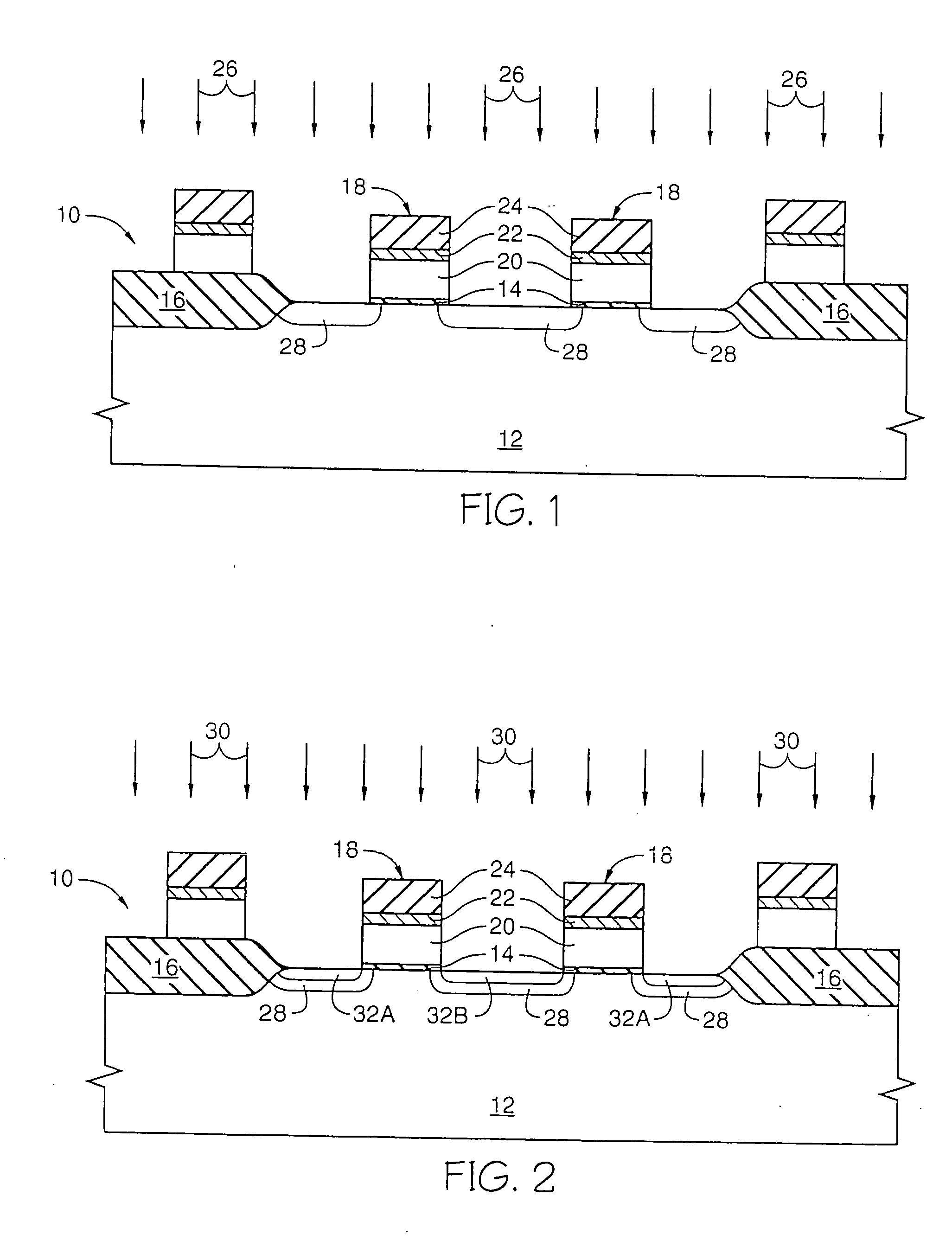
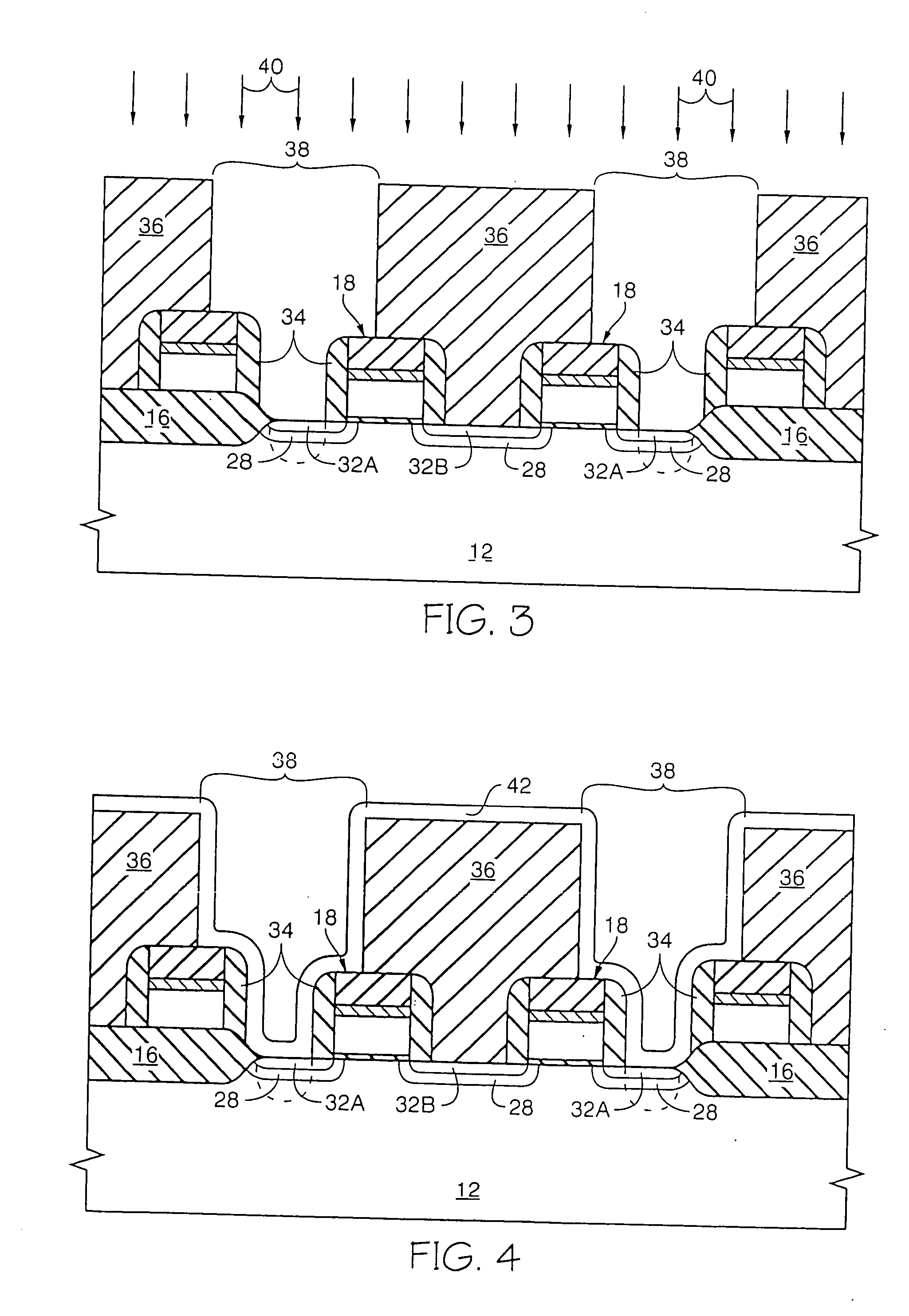
[0022] The present invention will be described in terms of Metal Oxide Semiconductor (MOS) technology which is currently the most commonly used integrated circuit technology. MOS generally refers to any integrated circuit in which Metal Oxide Semiconductor Field Effect Transistors (MOSFETs) are used. MOS integrated circuits are typically formed with a lightly doped p-type silicon substrate or a lightly doped n-type silicon substrate. The present invention will be described using lightly doped p-type silicon as the starting material, although the invention may be implemented with other substrate materials. If other substrate materials are used, then there may be corresponding differences in materials and structure of the device as is well known in the art.
[0023] The formation of integrated circuits includes photolithographic masking and etching. This process consists of creating a photolithographic mask containing the pattern of the component to be formed, coating the wafer with a l...
PUM
 Abstract
Description
Claims
Application Information