Electrostatic discharge mitigation structure and methods thereof using a dissipative capacitor with voltage dependent resistive material

a technology of resistive material and dissipative capacitor, which is applied in the incorporation of printed capacitors, emergency protective arrangements for limiting excess voltage/current, instruments, etc., can solve the problems of increased sensitivity to esd damage, esd damage from the worker to an electronic device can damage, and cannot eliminate esd damage, etc., to reduce esd damage and shield, and reduce emi/rfi

Inactive Publication Date: 2005-12-15
SOLECTRON
View PDF7 Cites 41 Cited by
  • Summary
  • Abstract
  • Description
  • Claims
  • Application Information

AI Technical Summary

Benefits of technology

[0005] The present invention relates to structures and methods to reduce ESD damage and shield against EMI and RFI. By placing one or more parallel plate capacitors adjacent an electronic device the invention places one or more capacitors in series with the current flowing through the electronic device when there is ESD. The capacitance acts as a capacitive voltage divider to the ESD. After the discharge, the dissipative characteristics of the lossy dielectric of the physical structure cause the transferred electrical energy to be converted to thermal energy. The structure can be also used to reduce EMI / RFI.

Problems solved by technology

Electrostatic discharge (ESD) from the worker to an electronic device can damage it.
Grounding the machines, the worker, the walls, and the floor as well as controlling humidity will help, but not eliminate ESD damage especially if the device is transported around the factories.
Sensitivity to ESD damage increases as electronic devices such as semiconductors shrink in size.
For example, if semiconductors have submicron size conductive channels, even tenths of a volt can cause a surge current that exceeds channel current capacity and fuses the channels.

Method used


Image

  • Electrostatic discharge mitigation structure and methods thereof using a dissipative capacitor with voltage dependent resistive material
  • Electrostatic discharge mitigation structure and methods thereof using a dissipative capacitor with voltage dependent resistive material
  • Electrostatic discharge mitigation structure and methods thereof using a dissipative capacitor with voltage dependent resistive material

Examples


Embodiment Construction

[0017] The following description includes the best mode of carrying out the invention. The detailed description is made for the purpose of illustrating the general principles of the invention and should not be taken in a limiting sense. The scope of the invention is best determined by reference to the claims.

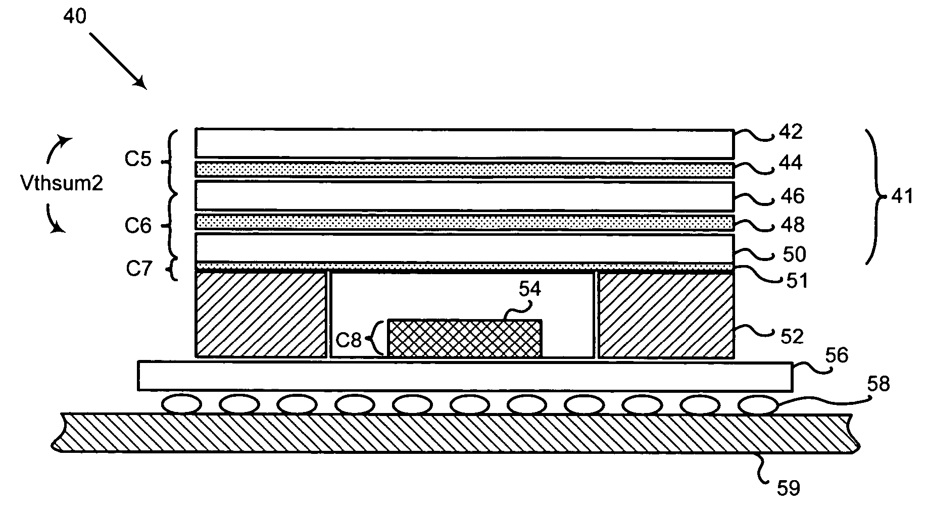
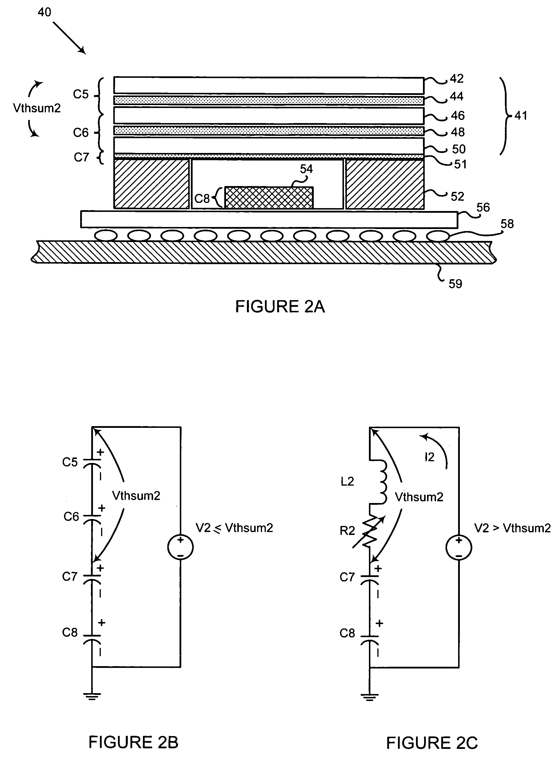
[0018] We assign each part, even if structurally identical to another part, a unique reference number wherever that part appears in the drawings. A dashed circle indicates a part of a figure that is enlarged in another figure. The reference number tied to the dashed circle indicates the figure showing the enlarged portion.

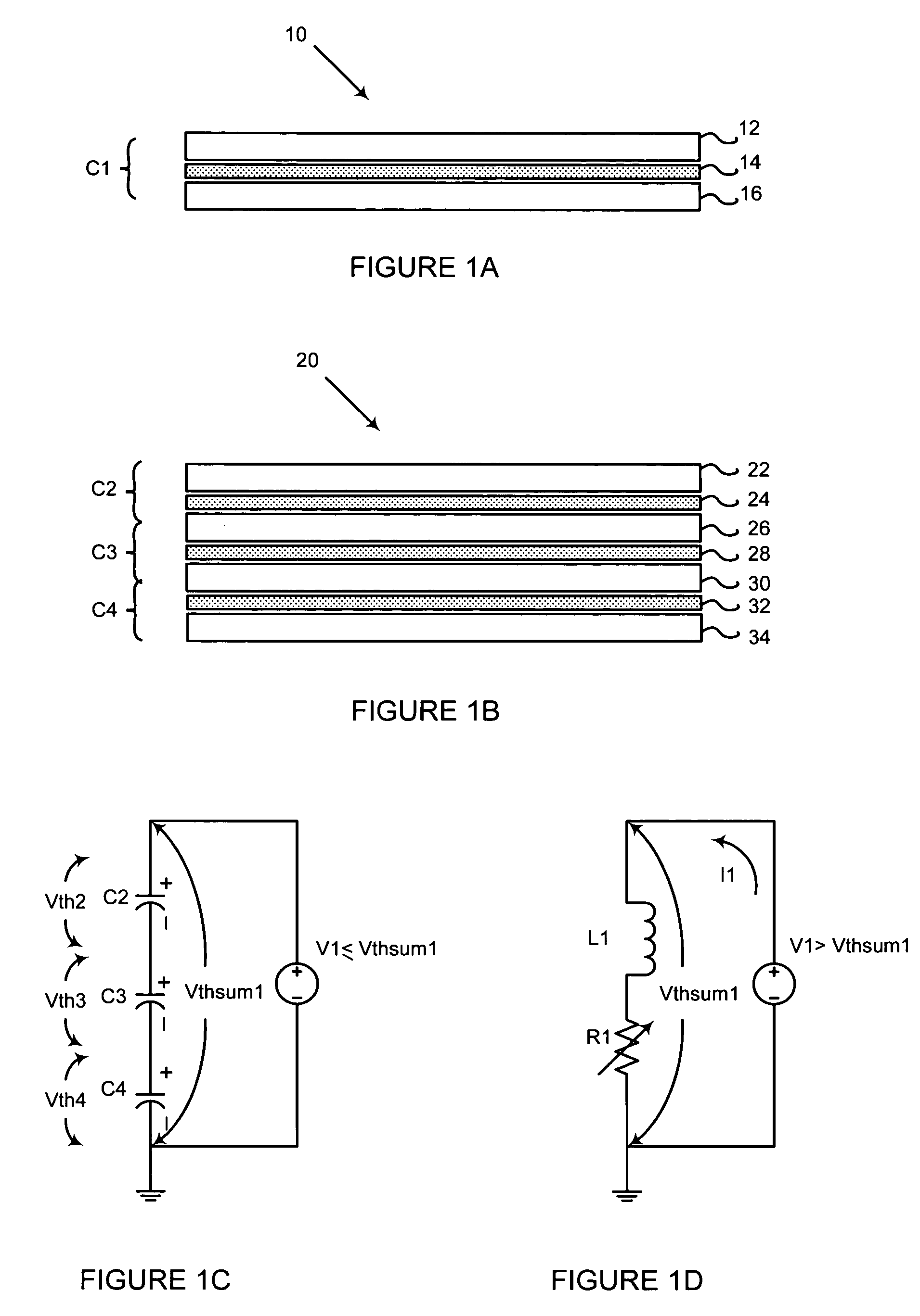
[0019]FIG. 1A illustrates a structure made of a parallel plate dissipative capacitor that will reduce ESD damage. In an embodiment, a structure 10 is a parallel plate dissipative capacitor C1 formed by sandwiching a dissipative dielectric layer 14 between a first conductive layer 12 and a second conductive layer 16.

[0020] In the embodiment, the dissipative d...


PUM


Abstract

The present invention relates to structures and methods that reduce ESD damage to electronic devices. In an embodiment, the structure is a parallel plate dissipative capacitor formed by sandwiching a dissipative dielectric layer between two conductive layers in series to the electronic device. The dissipative dielectric layer includes a nonconductive dielectric doped with a voltage dependent resistive material that defines a conductive threshold voltage. The structure functions as a voltage dependent resistor in response to an applied voltage such as an ESD surge voltage exceeding the defined conductive threshold voltage and dissipates the applied voltage into thermal energy before it can reach the electronic device and cause damage. The dissipative dielectric layer restores to a dielectric and the structure functions as a capacitor when the excess voltage is depleted that is drops below the defined conductive threshold voltage. In another embodiment, the structure is a parallel plate dissipative capacitors in series that enhances ESD mitigation through a capacitive voltage divider structure. The structures can be used in EMI/RFI shielding applications.

Description

BACKGROUND [0001] The present invention relates to structures and methods that reduce damage from electrostatic discharge and / or shield against electromagnetic and radio frequency interference. [0002] In electronic manufacturing, a worker may develop electrostatic charge from touching or rubbing surfaces as he works. Electrostatic discharge (ESD) from the worker to an electronic device can damage it. Grounding the machines, the worker, the walls, and the floor as well as controlling humidity will help, but not eliminate ESD damage especially if the device is transported around the factories. [0003] Sensitivity to ESD damage increases as electronic devices such as semiconductors shrink in size. For example, if semiconductors have submicron size conductive channels, even tenths of a volt can cause a surge current that exceeds channel current capacity and fuses the channels. [0004] It would be desirable to have structures and methods to reduce ESD damage especially during transportatio...

Claims


Application Information

Patent Timeline
Patent Type & Authority Applications(United States)
IPC IPC(8): H05K1/02H02H9/00H01L29/94H01L23/552H05K1/16H01L23/62
CPCH01L23/552H01L23/62H01L2924/15311H01L2924/16195H05K1/0254H05K1/162H01L2924/0002H01L2924/00
Inventor HOLLINGSWORTH, TOMMY D.
Owner SOLECTRON
Why Eureka
Try Eureka