Method of reducing ESD damage in thin film read heads which enables measurement of gap resistance

a thin film read head and gap resistance technology, applied in the field of thin film read head esd damage reduction devices, can solve problems such as potential difference across gap layers, dielectric breakdown, and electrical shorts at the location of breakdown, and achieve the effect of reducing esd damage to the sensor

Inactive Publication Date: 2005-09-20
HITACHI GLOBAL STORAGE TECH NETHERLANDS BV
View PDF5 Cites 10 Cited by
  • Summary
  • Abstract
  • Description
  • Claims
  • Application Information

AI Technical Summary

Benefits of technology

[0007]The present invention provides a device and method of reducing ESD damage to the sensor of the read head while enabling measurement of the first and second gap resistances. The first read gap layer can be considered to have a resistance RG1 between the first shield layer and one of the first and second lead layers and the second read gap layer can be considered to have a resistance RG2 between the second shield layer and one of the first and second lead layers. A short is provided via a plurality of resistors between a first node and each of the first and second shield layers wherein the plurality of resistors includes at least first and second resistors RS1 and RS2 and the first node is connected to either one of the first and second leads. A second node is located between the first and second resistors RS1 and RS2. An operational amplifier has first and second inputs connected to the first and second nodes respectively so as to be across the first resistor RS1 and has an output connected to the first node for maintaining the first and second nodes at a common voltage potential.

Problems solved by technology

The presence of this charge causes a potential difference across the gap layers.
When this voltage reaches a sufficiently high value, the dielectric breaks down, and electrical shorts can occur at the location of the breakdown.
Shorts between the sensor and the shields are detrimental to the operation of the head.
While this will provide protection against process-induced charging, it does not allow the ability to test for shield shorts due to other phenomena, such as pinholes in the gap dielectric.

Method used


Image

  • Method of reducing ESD damage in thin film read heads which enables measurement of gap resistance
  • Method of reducing ESD damage in thin film read heads which enables measurement of gap resistance
  • Method of reducing ESD damage in thin film read heads which enables measurement of gap resistance

Examples


first embodiment

of the Invention

[0038]A first embodiment 200 of the present invention is shown in FIG. 12 which shows the first and second lead layers 134 and 136 (L1 and L2) connected to the read sensor 74. The sensor 74 is shown as having a resistance RMR. FIG. 12 also shows the first and second shield layers S1 and S280 and 82 are shorted by a lead 202. First and second resistors 204 and 206 are connected across the second lead L2 and the first and second shield layers S1 and S2. With this arrangement the first read gap layer 76 has a resistance RG1 between the shield layers S1 and S2 and the second lead L2 and the second read gap layer 78 has a resistance RG2 between the shield layers S1 and S2 and the second lead L2. Alternatively, the first and second resistors 204 and 206 may be connected between the first and second shield layers S1 and S2 and the first lead layer L1. In this instance, the resistance RG1 would be the resistance between the shield layers S1 and S2 and the first lead layer L1...

second embodiment

of the Invention

[0040]FIG. 14 illustrates a second embodiment 300 of the present invention which is an improvement over the first embodiment 200 in FIG. 13. The embodiment 300 is the same as the embodiment 200 except for the following. The center point (CP) has two separate connections 302 and 304. The second lead L2 can be considered as a first node in the circuit and the connection 302 can be considered as a second node. An operational amplifier 306 has a first input 308 connected to the second lead L2 (first node) and a second input 310 connected to the first contact 302 (second node). The output 312 of the operational amplifier is connected to the second contact 304 which is located between the first contact 302 and the second resistor 206. The operational amplifier 306, which is configured as a unity gain buffer, is adjusted so that it drives the center point (CP) between the resistors 204 and 206 to the same potential as the second lead L2 (first node). As a result, there is z...

third embodiment

of the Invention

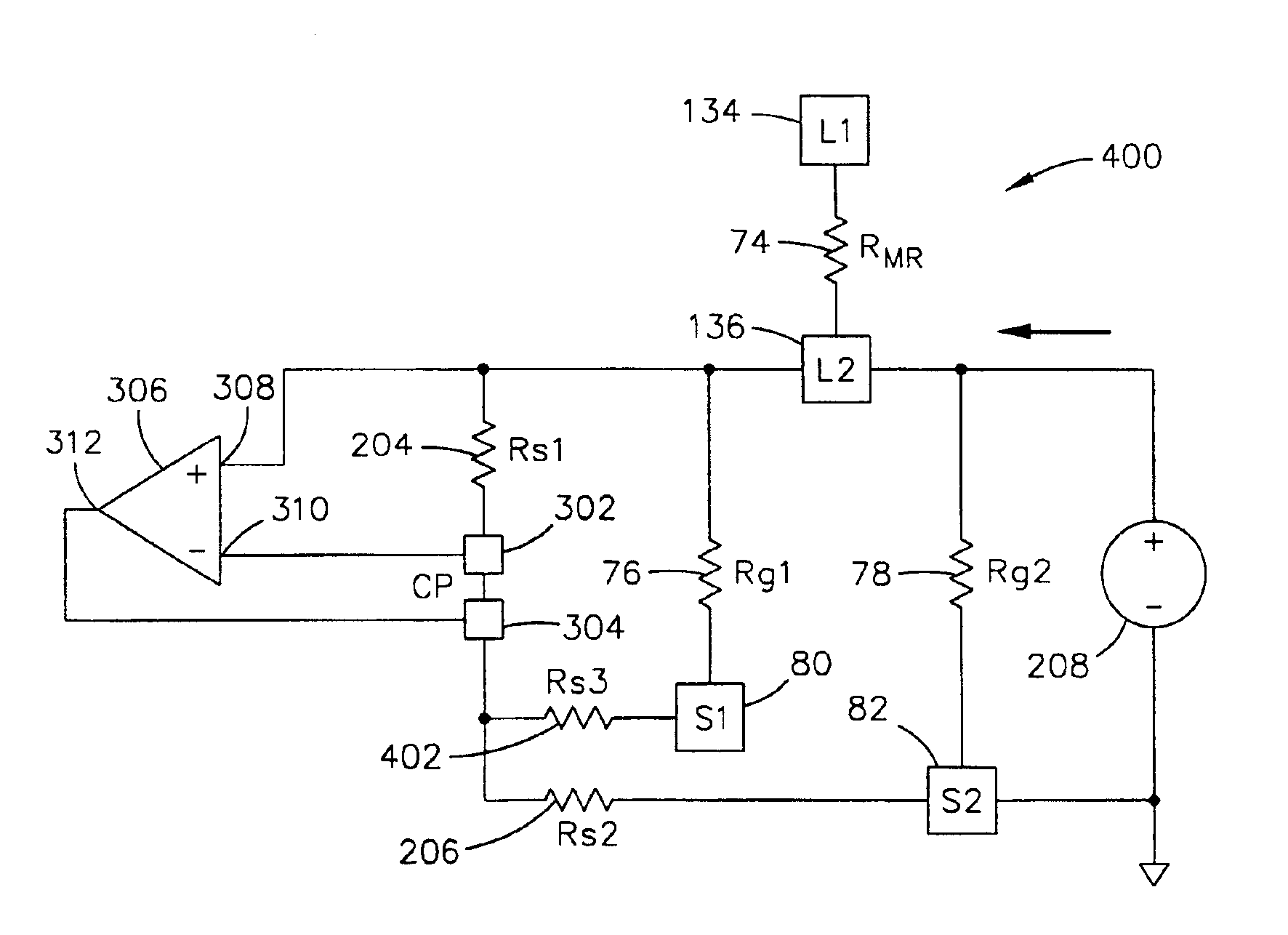
[0042]FIG. 15 shows a third embodiment 400 of the present invention which can measure the resistances RG1 and RG2 of the first and second gap layers 76 and 78 separately and is therefore an improvement over the embodiment 300 in FIG. 14. The embodiment 400 is the same as the embodiment 300 in FIG. 14 except for the following. The first and second shield layers S1 and S2 are no longer shorted together and a third resistor 402 having a resistance RS3 is connected between the center point (second node) and the first shield layer S1. The resistances RG1 and RG2 of the first and second gap layers 76 and 78 can now be determined separately. The resistance RG2 of the second gap layer 78 can be determined when the circuit tester 208 is connected across the second shield layer S2 and the second lead layer L2. Optionally, the resistance RG1 of the first read gap layer 76 can be determined by connecting the circuit tester 208 across the first shield layer S1 and the second lead...


PUM

PropertyMeasurementUnit
nonmagneticaaaaaaaaaa
resistance RG1aaaaaaaaaa
resistance RG2aaaaaaaaaa

Abstract

The present invention provides a method of manufacturing a magnetoresistive read head which reduces electrostatic discharge and allows measurement of gap resistances in the head.

Description

[0001]This is a division of application Ser. No. 09 / 753,804 filed Jan. 2, 2001, now U.S. Pat. No. 6,678,127.BACKGROUND OF THE INVENTION[0002]1. Field of the Invention[0003]The present invention relates to a device for reducing electrostatic discharge (ESD) damage in thin film read heads which enables measurement of gap resistances and, more particularly, to such a device and method wherein the resistance of first and second gap layers can be measured in parallel or the resistance of each of the first and second gap layers can be measured separately.[0004]2. Description of the Related Art[0005]The heart of a computer is a magnetic disk drive which includes a rotating magnetic disk, a slider that has read and write heads, a suspension arm above the rotating disk and an actuator arm that swings the suspension arm to place the read and write heads over selected circular tracks on the rotating disk. The suspension arm biases the slider into contact with the surface of the disk when the d...

Claims


Application Information

Patent Timeline
Patent Type & Authority Patents(United States)
IPC IPC(8): G11B5/455G11B5/40G11B33/00G11B5/00G11B33/10G11B5/33G11B5/39
CPCG11B5/40G11B5/455B82Y10/00Y10T29/49039Y10T29/49036G11B5/33G11B5/3967G11B33/10G11B2005/0013Y10T29/49078Y10T29/49044Y10T29/49071Y10T29/49032Y10T29/49043Y10T29/49073
Inventor HSIAO, RICHARDJARRATT, JAMES D.KLAASSEN, EMO HILBRANDMCFADYEN, IAN ROBSONMORAN, TIMOTHY J.
Owner HITACHI GLOBAL STORAGE TECH NETHERLANDS BV
Why Eureka
Try Eureka