Display device using printed circuit board as substrate of display panel

Inactive Publication Date: 2005-12-15
LG CHEM LTD
View PDF7 Cites 17 Cited by
  • Summary
  • Abstract
  • Description
  • Claims
  • Application Information

AI Technical Summary

Benefits of technology

[0018] According to the present invention, the electric signal of the driving circuit is directly applied to the electrode through the via hole of t

Problems solved by technology

The above problem may occur in various display devices in addition to the ECD.
Accordingly, the resp

Method used


Image

  • Display device using printed circuit board as substrate of display panel
  • Display device using printed circuit board as substrate of display panel
  • Display device using printed circuit board as substrate of display panel

Examples


Embodiment Construction

[0028] Reference will now be made in detail to the preferred embodiment of the present invention, examples of which are illustrated in the accompanying drawings. Wherever possible, the same reference numbers will be used throughout the drawings to refer to the same or like parts.

[0029]FIG. 3 is a schematic view illustrating a structure of a display device using a PCB as a substrate of a display panel according to a preferred embodiment of the present invention.

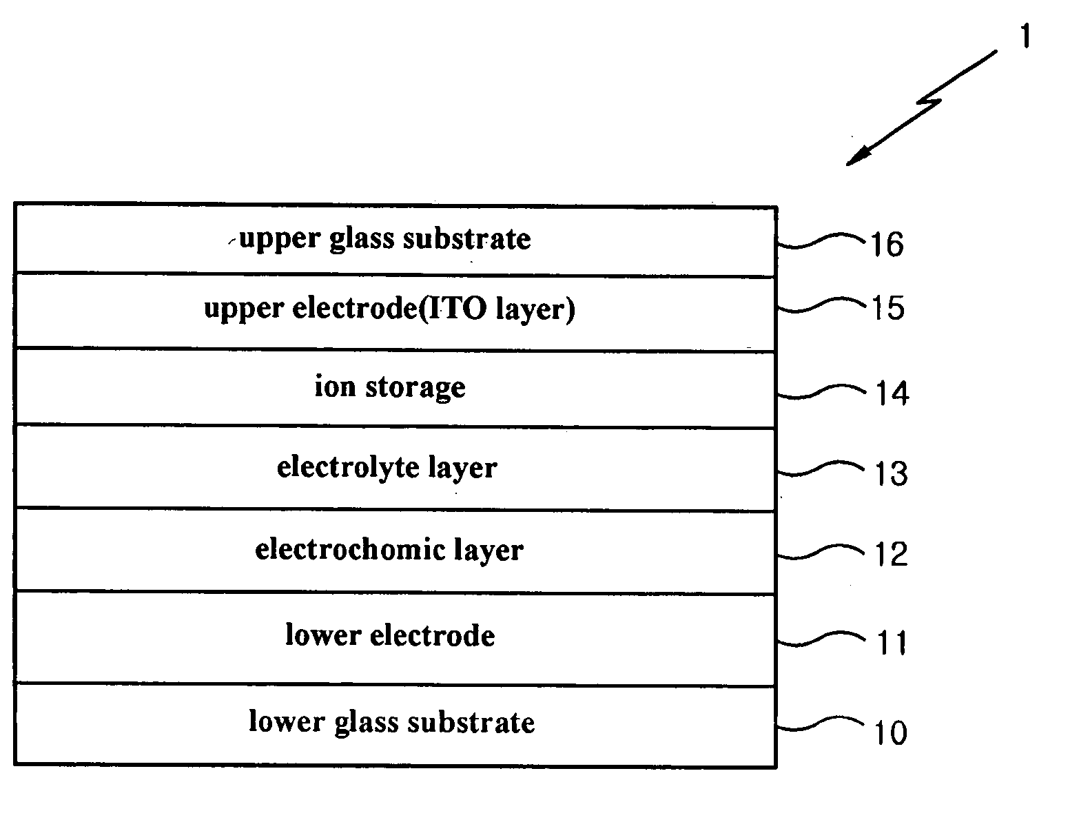
[0030] Referring to FIG. 3, a display panel 20 of an ECD is mounted on a PCB 20. The PCB 30 is a double-side PCB provided at a lower surface thereof with a driving circuit section 36. An electric diving signal generated from the driving circuit section 36 is directly applied to a lower electrode 21 of the display panel by way of a wiring 34 and a via hole 32.

[0031] Electronic parts of the driving circuit section 36 can be formed in a separate PCB such that they are electrically connected to the wiring 34 without directly ma...


PUM


Abstract

Disclosed is a display device using a printed circuit board (PCB) as a substrate of a display panel. The display device includes the PCB formed with a via hole, a display panel having an electrode aligned adjacent to one side of the via hole formed in the PCB in order to apply an electric signal to a pixel or a segment, a driving circuit section for applying an electric signal to the display panel, and a wiring section for electrically connecting the electrode of the display panel to the driving circuit section through the via hole. The electric signal of the driving circuit is directly applied to the lower electrode through the via hole of the PCB, so the length of the electrode line used for wiring can be significantly reduced, thereby improving the response speed of the display device.

Description

BACKGROUND OF THE INVENTION [0001] 1. Field of the Invention [0002] The present invention relates to a display device using a printed circuit board (PCB) as a substrate of a display panel. More particularly, the present invention relates to a display device capable of improving the response speed and image quality thereof by directly connecting pixels or segments of a display panel to a driving circuit through a via hole formed in a PCB. [0003] 2. Description of the Prior Art [0004] Generally, display devices are classified into emissive display, such as CRTs, PDPs, LEDs, or OLEDs, and non-emissive display, such as LCDs. The emissive display represents the high response speed, but the image becomes faint in a bright place. In contrast, the non-emissive display represents the low response speed although it can clearly display the image in the bright place. [0005] Among other things, an electrochromic display (ECD) is a non-emissive display, such as an LCD, capable of adjusting the co...

Claims


Application Information

Patent Timeline
IPC IPC(8): G02F1/13G02F1/1345G02F1/153G02F1/155H05K1/16
CPCG02F1/1345G02F1/13452H05K1/16G02F1/155G02F2201/42G02F1/1533
Inventor PARK, KEE YONG
Owner LG CHEM LTD
Why Eureka
Try Eureka