Package design and method for electrically connecting die to package

Inactive Publication Date: 2005-11-17
MINDSPEED TECH INC
View PDF4 Cites 13 Cited by
  • Summary
  • Abstract
  • Description
  • Claims
  • Application Information

AI Technical Summary

Benefits of technology

[0021] In one embodiment the wirebond connects to a bonding pad prepared on the conductive layer that is accessed through the bonding hole and bonding pad may be prepared on the conductive layer using a gold deposition. In addition, in one embodiment, the device further comprises one or more solder bumps or pins elect

Problems solved by technology

Because of the close proximity of the wirebonds and the required flexibility of the wirebonds, during the packaging of the die the wirebonds often suffer from a phenomenon known as wire-sweep.
This will yield the chip unusable and is a significant cause of product rejection during the manufacturing process.
This is a drawback associated with prior art methods that utilize a design that extends the wirebond to a distant bonding pad.
Another drawback associated with this arrangement

Method used


Image

  • Package design and method for electrically connecting die to package
  • Package design and method for electrically connecting die to package
  • Package design and method for electrically connecting die to package

Examples


Example

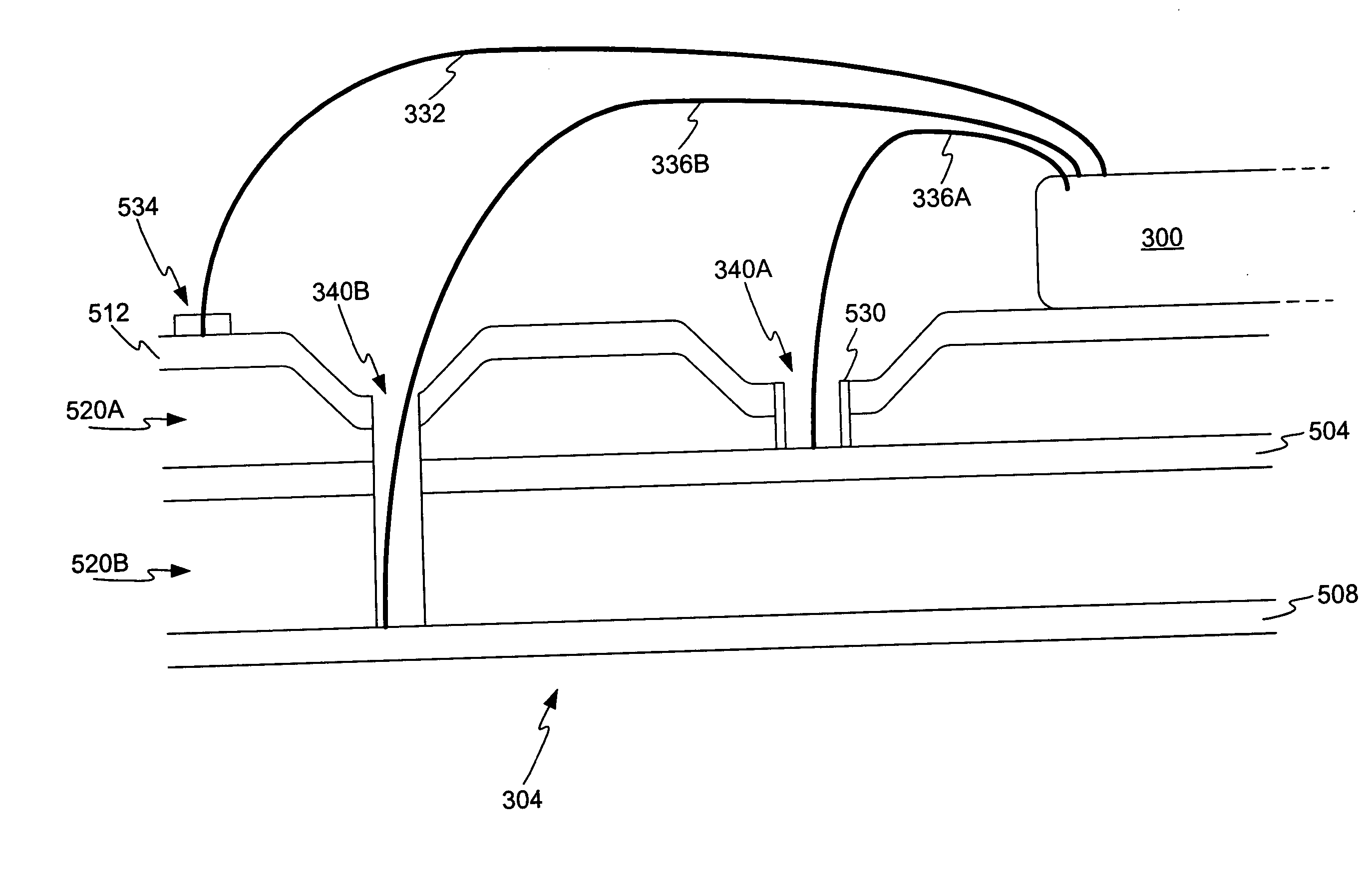
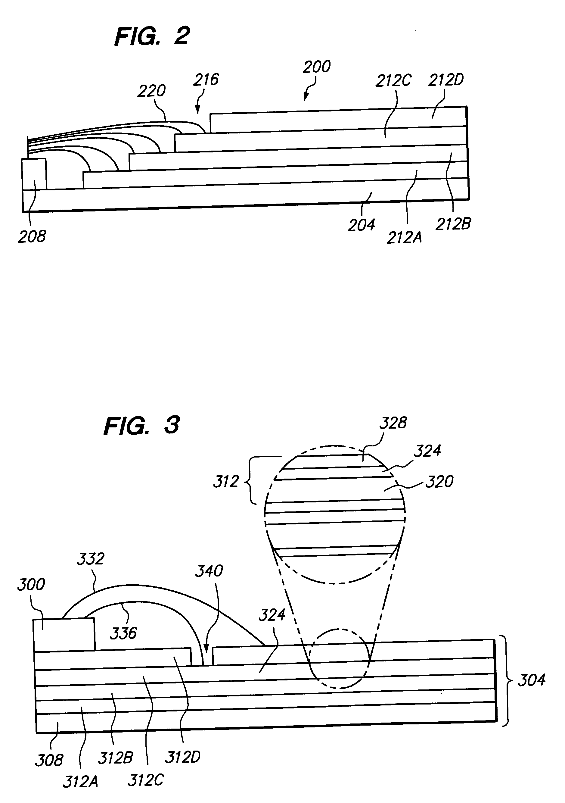
[0030] One proposed solution to the prior art problem of excessive wirebond lengths is to configure a package as shown in FIG. 2. FIG. 2 illustrates a cut-away side view of a package. As shown, a laminated package 200 is configured with a base layer 204 that supports the die 208 and one or more layers 212A, 212B, 212C, 212D that are built up over the base layer 204. The edges of the layers 212 near the die 208 are stair-stepped and the exposed step of each layer is configured with a wirebond pad 216. This arrangement is also known as wirebond tiers. The wirebonds extend from the die and connect to the bonding pads 216. The stair-stepped arrangement of the package, as shown, allows for shorter wirebonds 220 because the bonding pads 216 on the package may be placed more closely together and, due to the stair step configuration, wire-sweep is less likely.

[0031] This configuration is, however, more difficult to manufacture because, each layer 212 that is placed on the base layer 204 mu...


PUM


Abstract

A method and apparatus for electrically connecting a die to a package while reducing the length of wirebonds. This in turn reduces wire-sweep and the cost of manufacture. To reduce the length of the wirebonds, bonding holes are created through an insulating layer of the package to expose a conductive layer. A wirebond connects through the bonding hole to a conductive layer that is exposed by the hole. The attachment point for the wirebond on the conductive layer may be prepared to serve as a bonding pad. Using this technique the prior art method utilized a bonding pad on the top surface of the inner surface of the package, which electrically connects through a trace to a via, which in turn electrically connects to a conductive layer may be avoided thereby allowing for closer spacing of radially concentric rows of attachment points on the package around the die.

Description

FIELD OF THE INVENTION [0001] The invention relates to semiconductor design and manufacture and, in particular, to a method and apparatus for package construction to enable electrical connection between a die and a package. RELATED ART [0002] There exists a continuing demand for electronic devices that have greater functionality and speed. As such there has been, and continues to be, great strides in the development of new integrated circuit technologies that allow circuit designers to meet these needs. For example, electronic circuits increasingly operate at higher speeds and enjoy reductions in size as compared to circuits of a few years ago. [0003] By way of background, an integrated circuit is often referred to as an electronic “chip” and it often comprises numerous subparts. In particular, a die or integrated circuit, which contains or comprises one or more circuits, is housed within a package that protects and secures the die. The die often comprises one or more metallic layer...

Claims


Application Information

Patent Timeline
IPC IPC(8): H01L21/60H01L23/04H01L23/498
CPCH01L23/49827H01L23/49838H01L2224/48233H01L2924/01033H01L2924/00014H01L2924/3025H01L2924/3011H01L2924/1517H01L2924/15153H01L2924/14H01L2924/014H01L2924/01082H01L2924/01079H01L2924/01078H01L2924/01006H01L24/45H01L24/48H01L24/49H01L24/85H01L2224/45144H01L2224/48091H01L2224/48227H01L2224/48228H01L2224/484H01L2224/48599H01L2224/49109H01L2224/49171H01L2224/85H01L2924/01005H01L2224/78H01L2924/00
Inventor LYNCH, MARKHASHEMI, SEYED HASSAN
Owner MINDSPEED TECH INC
Why Eureka
Try Eureka