Semiconductor device having a plurality of semiconductor constructs

Inactive Publication Date: 2007-07-12
THE RGT OF THE UNIV OF MICHIGAN +1
View PDF3 Cites 14 Cited by
  • Summary
  • Abstract
  • Description
  • Claims
  • Application Information

AI Technical Summary

Benefits of technology

[0034]According to this invention, since all the upper surfaces of the plurality of external connection electrodes are exposed on the one semiconductor construct and on the insulating film, the electrical connection wiring lines are mainly in a thickness direction of the semiconductor construct. Thus, the length of the wiring lines is red

Problems solved by technology

The conventional semiconductor device described above has the following problems due to the connection by the bonding wires.
That is, the diameter of the bonding wire is generally small because costs increase if the diameter of the bonding wire made of gold is relatively large, and the impedance of the bonding wire is high because the bonding wire is relative

Method used


Image

  • Semiconductor device having a plurality of semiconductor constructs
  • Semiconductor device having a plurality of semiconductor constructs
  • Semiconductor device having a plurality of semiconductor constructs

Examples


Example

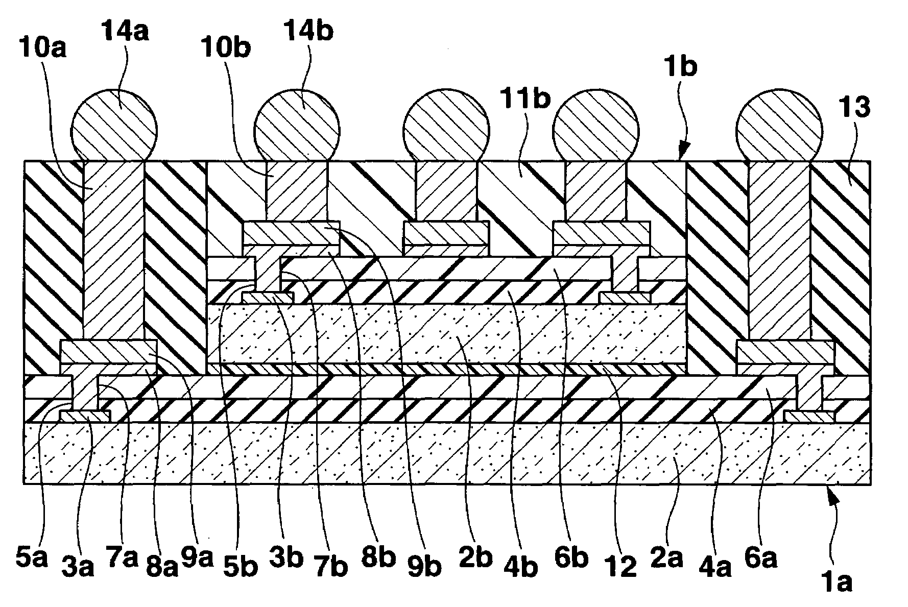
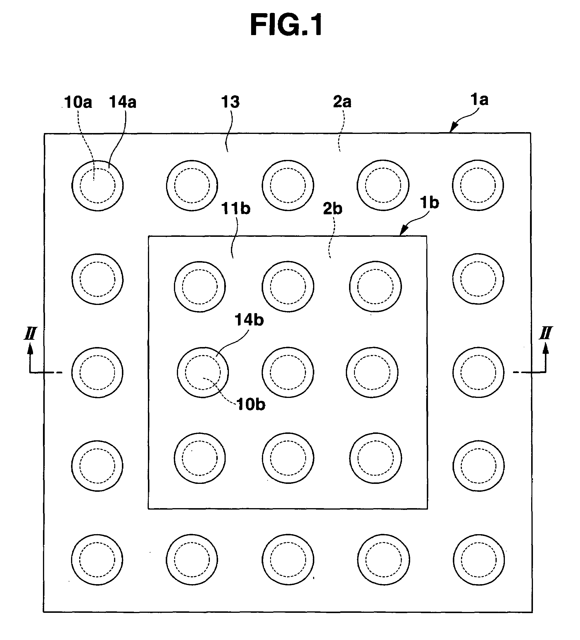
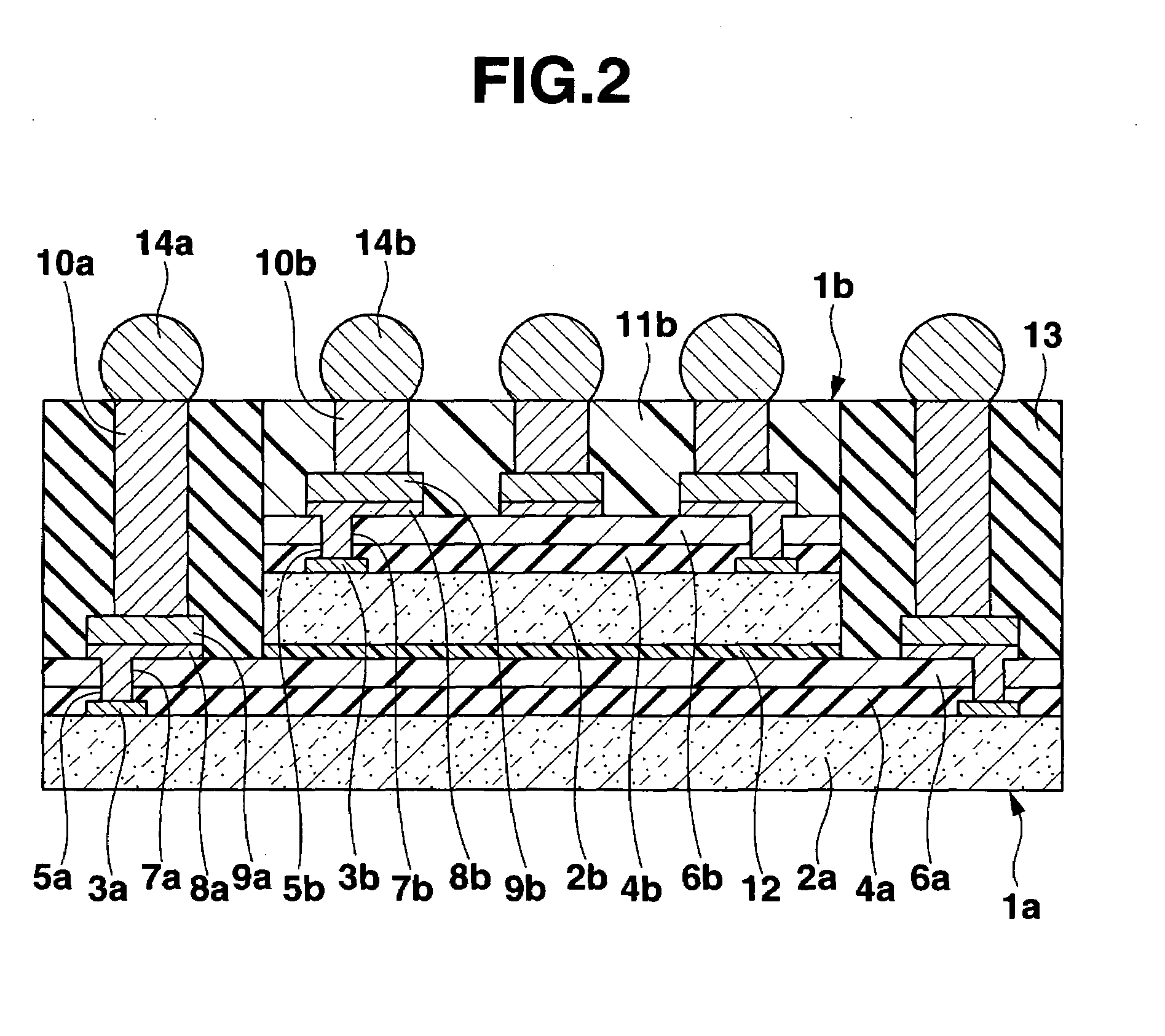
[0053]FIG. 1 is a plan view of a semiconductor device as a first embodiment of this invention, and FIG. 2 is a sectional view along the line II-II of FIG. 1. This semiconductor device includes a first planar square semiconductor construct 1a, and a second planar square semiconductor construct 1b stacked on the first semiconductor construct 1a. The first and second semiconductor constructs 1aand 1b are different in a planar-size but are much the substantially same in basic configuration, and are so-called chip size packages (CSPs) in general.

[0054]The first and second semiconductor constructs 1aand 1b respectively include planar square silicon substrates (semiconductor substrates) 2a and 2b. The planar-size of the second silicon substrate 2b is somewhat smaller than the planar-size of the first silicon substrate 2a. Integrated circuits (not shown) having a predetermined function are provided on the upper surfaces of the silicon substrates 2a and 2b, and a plurality of first and secon...

Example

Second Embodiment

[0074]FIG. 12 is a sectional view of a semiconductor device as a second embodiment of this invention. This semiconductor device is different from the semiconductor device shown in FIG. 2 in that a semiconductor construct having no second sealing film 11b is used in a second semiconductor construct 1b, and in that an insulating film 13 is directly provided on the upper surface of a protective film 6b including a second wiring line 9b so that the upper surface of this insulating film 13 is flush with the upper surfaces of second columnar or bump electrodes 10b.

[0075]Next, one example of a method of manufacturing this semiconductor device will be described. First, after the step shown in FIG. 6, adhesive bonding layers 12 fixedly attached to the lower surfaces of silicon substrates 2b of a plurality of semiconductor constructs 1b are adhesively bonded to the centers of the areas on the upper surface of a protective film 6a on a silicon substrate 2a in a wafer state wh...

Example

Third Embodiment

[0077]FIG. 15 is a sectional view of a semiconductor device as a third embodiment of this invention. The great differences between this semiconductor device and the semiconductor device shown in FIG. 2 are that a semiconductor construct having a first sealing film 11a is used as a first semiconductor construct 1a, and that first and second upper layer wiring lines 17a and 17b, upper layer columnar or bump electrodes (third columnar electrodes) 18a and 18b, an overcoat film 19, solder balls 14a and 14b, etc. are provided on a second semiconductor construct 1b and an insulating film 13.

[0078]That is, the first semiconductor construct 1a has a structure in which the first sealing film 11a is provided on the upper surfaces of a protective film 6a and first wiring lines 9a so that the upper surface of the first sealing film 11a is flush with the upper surfaces of first columnar electrodes 10a. In this case, the height of the first columnar electrode 10a is somewhat smalle...


PUM


Abstract

A semiconductor device includes a plurality of semiconductor constructs, each of the semiconductor constructs including a semiconductor substrate and external connection electrodes provided on an upper surface of the semiconductor substrate. The semiconductor substrates of the semiconductor constructs are different in a planar-size. The plurality of semiconductor constructs are stacked from bottom to top in descending order of planar-sizes of the semiconductor substrates included in the plurality of semiconductor constructs. An insulating film at least is provided around one semiconductor construct disposed on the top of the plurality of semiconductor constructs and on another semiconductor construct disposed under the one semiconductor construct. Each of the upper surfaces of the plurality of external connection electrodes is exposed from the one semiconductor construct and from the insulating film.

Description

CROSS-REFERENCE TO RELATED APPLICATIONS[0001]This application is based upon and claims the benefit of priority from prior Japanese Patent Application No. 2006-002017, filed Jan. 10, 2006, the entire contents of which are incorporated herein by reference.BACKGROUND OF THE INVENTION[0002]1. Field of the Invention[0003]This invention relates to a semiconductor device in which a plurality of semiconductor constructs are stacked.[0004]2. Description of the Related Art[0005]In a conventional semiconductor device, a first semiconductor construct is stacked on a base board, and a second semiconductor construct having a planar-size smaller than that of the first semiconductor construct is stacked on a part of the first semiconductor construct. A plurality of external connection electrodes are provided in a peripheral area of the upper surface of the first semiconductor construct which is exposed without being covered by the second semiconductor construct, and a plurality of external connecti...

Claims


Application Information

Patent Timeline
IPC IPC(8): H01L23/48
CPCH01L23/5389H01L2225/06568H01L24/82H01L2224/24226H01L2924/01013H01L2924/01029H01L2924/01078H01L2924/01079H01L2924/14H01L2924/15311H01L2924/3011H01L2924/01005H01L2924/01006H01L2924/01023H01L2924/01033H01L2924/014H01L24/24H01L23/3114H01L24/94H01L24/97H01L2224/12105H01L2224/32145H01L2224/73267H01L2224/94H01L2224/97H01L2224/83
Inventor MIHARA, ICHIRO
Owner THE RGT OF THE UNIV OF MICHIGAN
Why Eureka
Try Eureka