

Circuit interface device
- Summary
- Abstract
- Description
- Claims
- Application Information
AI Technical Summary
Benefits of technology
Problems solved by technology
Method used
Image

Examples
first embodiment
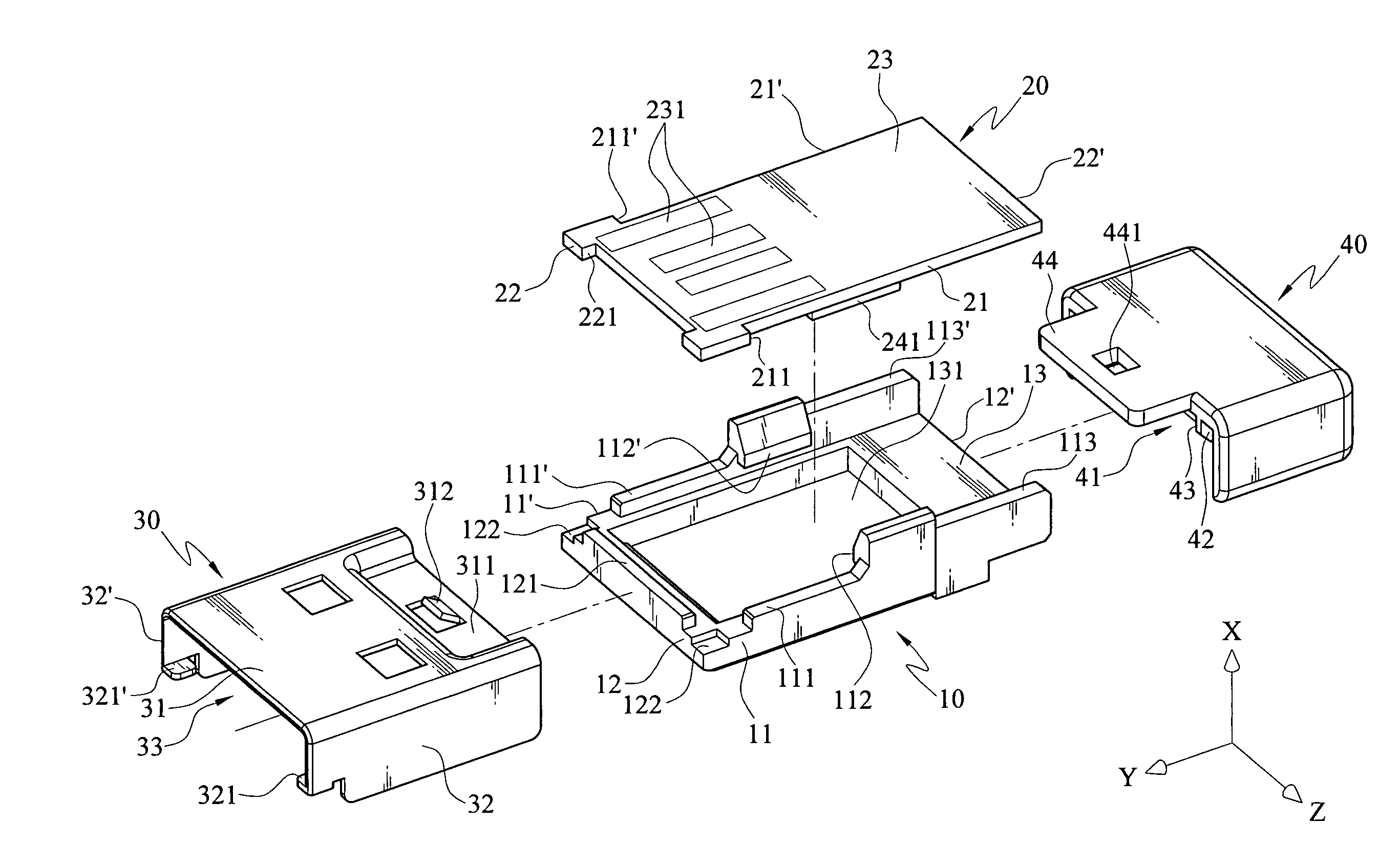
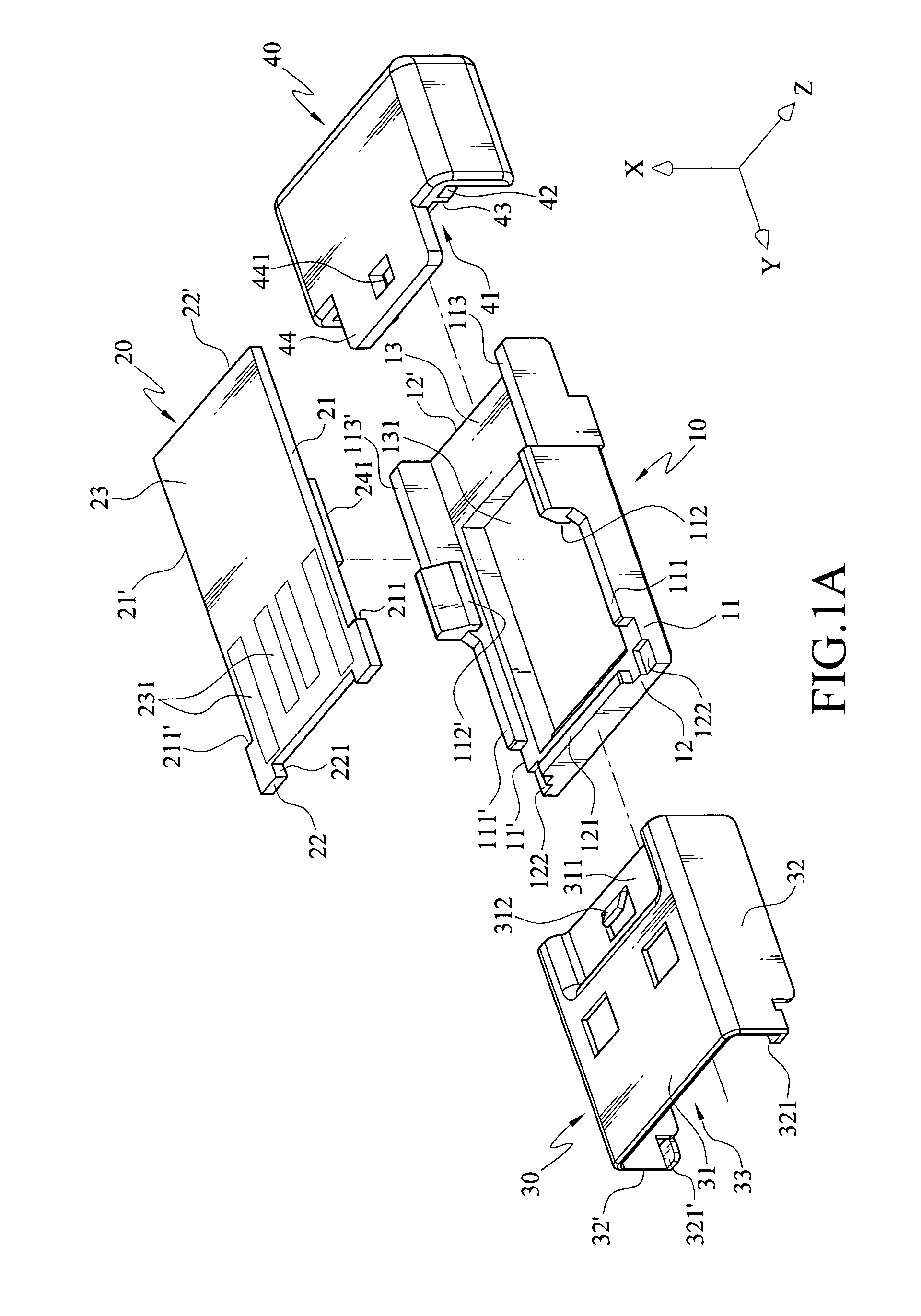
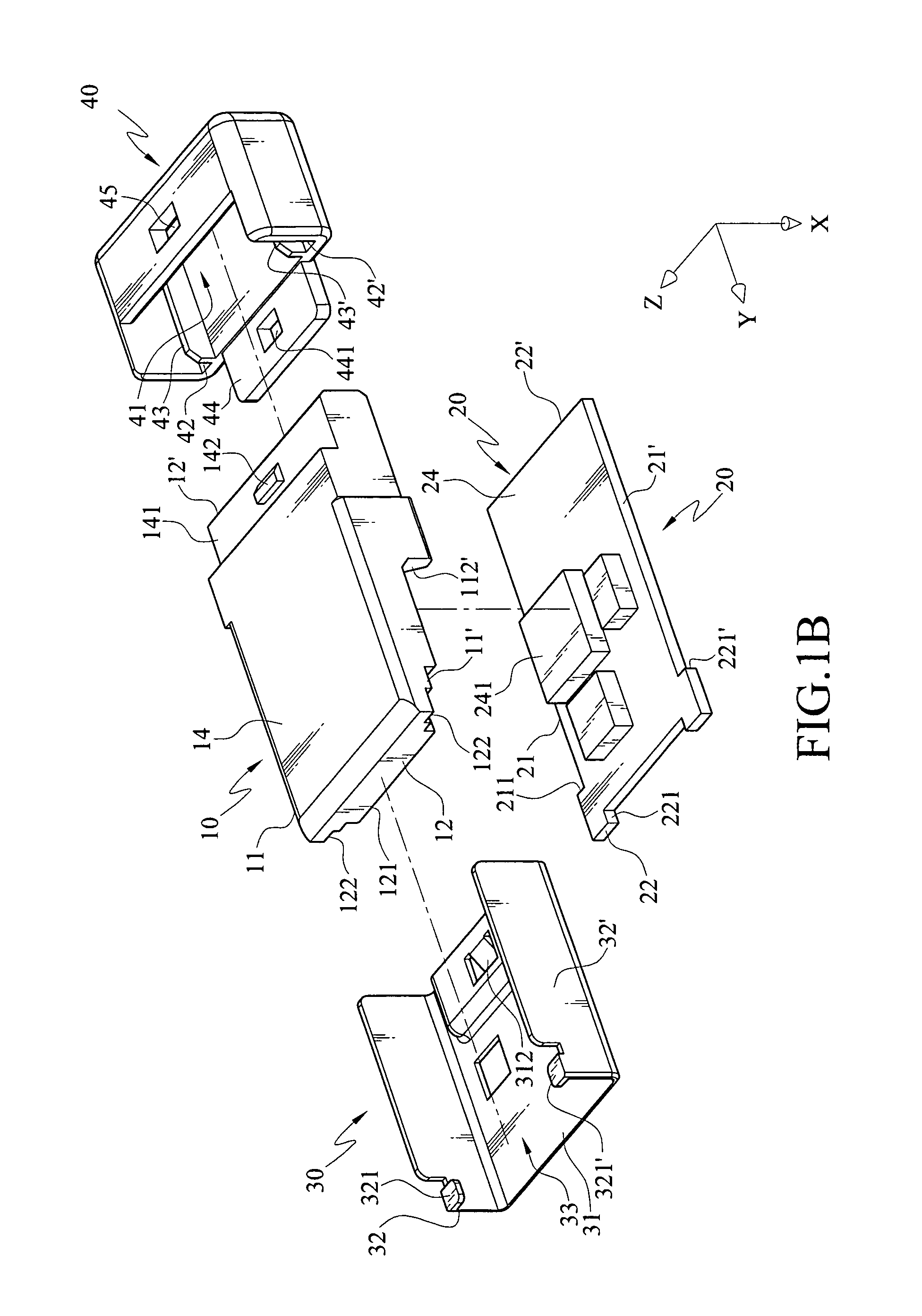
[0036]FIGS. 2A to 2C are schematic views of the assembly process according to the present invention. When the circuit board 20 is secured by the assembly plane 13 of the circuit board cover 10 along the X-axis direction, the first insertion block 121 and the second insertion blocks 111 and 111′ of the circuit board cover 10 are inserted into the first insertion groove 221 and the second insertion grooves 211 and 211′ of the circuit board 20 respectively. The side surface 24 of the circuit board 20 is flatly attached onto the assembly plane 13, and the electronic element 241 of the second side surface 24 is accommodated inside the accommodation groove 131 opened on the assembly plane 13. The circuit board 20 is tightly snapped and positioned by the hooks 112 and 112′ of the circuit board cover 10, so as to prevent the circuit board 20 from being detached from the circuit board cover 10 in the X-axis direction again.
[0037]Hence, after the circuit board 20 is mounted on the assembly pl...
second embodiment
[0048]FIGS. 6A to 6C are schematic views of motions for assembling the present invention to a peripheral input device. The circuit interface device according to the present invention may be assembled onto a peripheral input device 50, such as a mouse and a keyboard. In the following embodiment, a wireless mouse is taken for example, but the present invention is not limited thereto.
[0049]A sliding slot 52 is mainly disposed in a bottom surface 51 of the peripheral input device 50, and a T-shaped slide rail 55 is disposed at the end of the sliding slot 52. The height and width of the slide rail 55 are slightly smaller than those of the socket 33, and a rail slot 56 is formed at the two opposite sides of the slide rail 55.
[0050]Hence, when the circuit board cover 10 is inversed and placed into the sliding slot 52, the opening 34 opened in the base plate 31 of the connector cover 30 is towards the slide rail 55, and the circuit board cover 10 is pushed to move towards the slide rail 55,...
PUM
 Abstract
Description
Claims
Application Information