Multi-level power supply system for a complementary metal oxide semiconductor circuit

a technology of complementary metal oxide semiconductors and power supply systems, applied in emergency protective arrangements for limiting excess voltage/current, instruments, liquid/fluent solid measurement, etc., can solve problems such as high current flow from power supply to ground, inadvertent creation of extra devices, and damage to other circuits

Active Publication Date: 2005-12-15
GLOBALFOUNDRIES US INC
View PDF1 Cites 6 Cited by
  • Summary
  • Abstract
  • Description
  • Claims
  • Application Information

AI Technical Summary

Benefits of technology

[0012] These and other objects are achieved by a method for managing a multi-level power supply. The method includes comparing a voltage level (Vs1) of a lower voltage supply bus to a voltage level (Vs2) of a higher voltage supply bus, and routing current from said lower voltage supply bus to said higher voltage supply bus if Vs2<Vs1. The lower and higher voltage supply busses provide power to a CMOS circuit. The method prevents a latch-up of the CMOS circuit.

Problems solved by technology

During manufacturing, extra devices may be inadvertently created.
If the thyristor is connected between a power supply and an electrical ground, forward biasing of the p-n junction turns on the parasitic pnp and npn devices, which results in a high current flow from power supply to ground.
As a result of such high current, other circuits can be damaged, e.g., a melt down of metal wires.
A CMOS circuit built on a bulk silicon wafer is susceptible to latch-up.
Once latch-up occurs, not only may circuits cease to function, but the latch-up may also induce catastrophic failure from joule heating.
To power-on a system having multiple-voltage supplies, if one supply is ramped up faster (or slower) than another, it is possible that some p-n junctions may be unintentionally forward biased, and the system could enter the latch-up situation.
During power-on, if the higher voltage supply is ramped up more slowly than the lower voltage supply, a p-type source / drain junction may be forward biased to an n-type body, which could result in a latch-up, especially if guard rings are not installed.
However, in order to avoid latch-up, the sharing of wells is often prohibited.

Method used


Image

  • Multi-level power supply system for a complementary metal oxide semiconductor circuit
  • Multi-level power supply system for a complementary metal oxide semiconductor circuit
  • Multi-level power supply system for a complementary metal oxide semiconductor circuit

Examples


Embodiment Construction

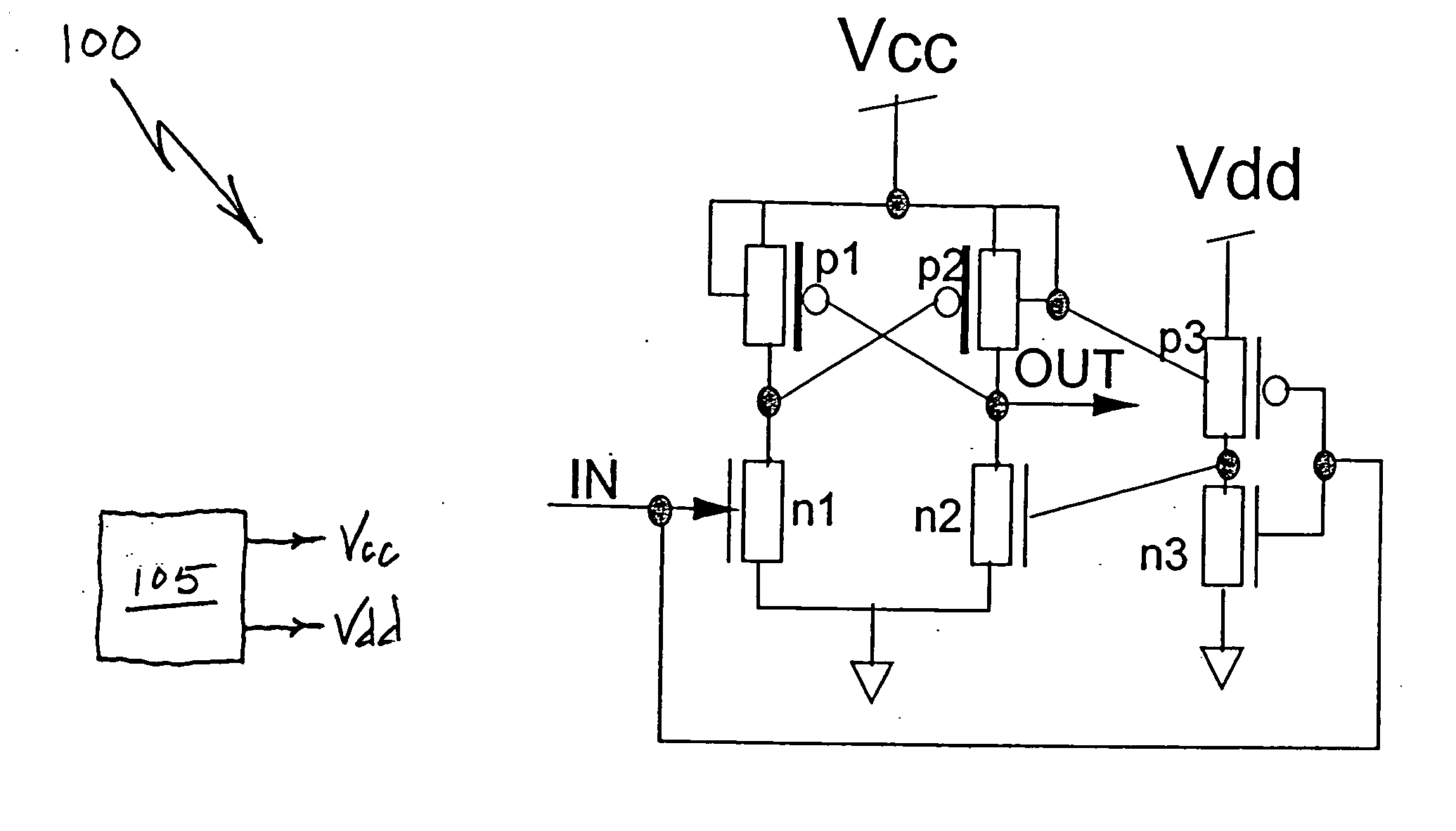
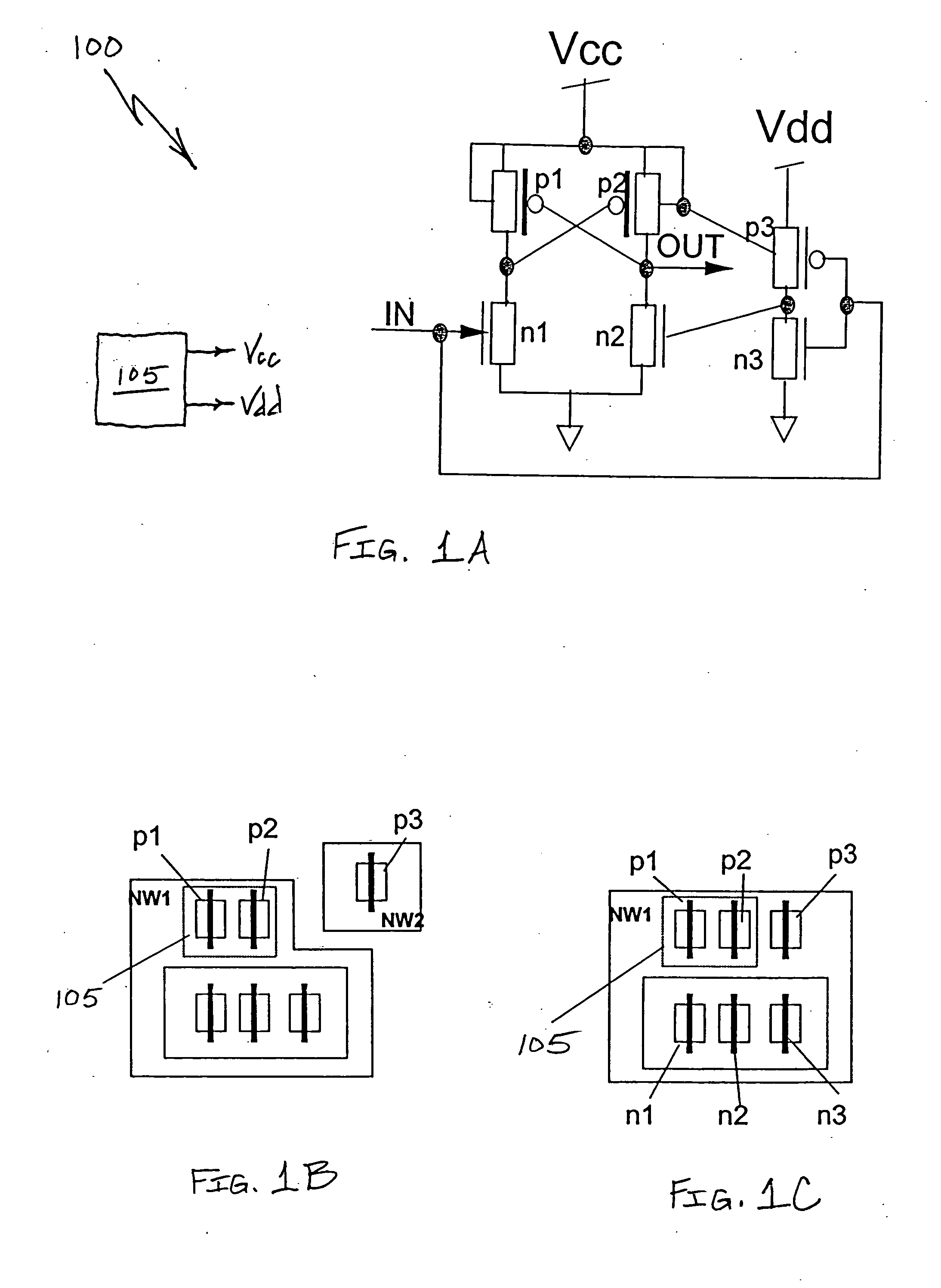
[0022] A power supply switch system utilizes a power switch to, under certain circumstances, route current from a lower voltage supply bus to a higher voltage supply bus. More specifically, if the higher voltage supply bus is not ready, e.g., is at a lower voltage level than that of the lower voltage supply bus, the power supply switch system routes current from the lower voltage supply bus to the higher voltage supply bus, thus avoiding latch-up of a CMOS device that is being powered by the voltage supply busses.

[0023] A voltage sensor, e.g., a comparator, is associated with the switch module. The comparator senses voltage levels on the supply busses and, based on a relationship between the voltage levels, determines “ON / OFF” states of the power switch. When the higher voltage supply bus is not available or is not ready, the switch is turned ON so that current is routed from the lower voltage supply bus to the higher voltage supply bus. The current continues until the higher volta...


PUM


Abstract

There is provided a method for managing a multi-level power supply. The method includes comparing a voltage level (Vs1) of a lower voltage supply bus to a voltage level (Vs2) of a higher voltage supply bus, and routing current from the lower voltage supply bus to the higher voltage supply bus if Vs2<Vs1. The lower and higher voltage supply busses provide power to a complementary metal oxide semiconductor (CMOS) circuit. The method prevents a latch-up of the CMOS circuit. There is also provided a circuit that employs the method.

Description

BACKGROUND OF THE INVENTION [0001] 1. Field of the Invention [0002] The present invention relates to a multi-level power supply, and more particularly, to a technique of managing a multi-level power supply to avoid a latch-up of a complementary metal oxide semiconductor (CMOS) circuit. [0003] 2. Description of the Related Art [0004] A semiconductor integrated circuit may include numerous active and passive devices. For example, the circuit may include active devices such as transistors, diodes, and thyristors, and passive devices such as capacitors, resistors and inductors. During manufacturing, extra devices may be inadvertently created. These extra devices are referred to as parasitic devices. The parasitic devices are not usually turned on during normal operation of the circuit, and current gain of parasitic pnp and npn bipolar transistors is normally very small. [0005] However, in some circumstances, such as during a power-on period, the parasitic devices can be activated. This ...

Claims


Application Information

Patent Timeline
Patent Type & Authority Applications(United States)
IPC IPC(8): G06F1/26G11C5/14G11C11/4074H02H7/00
CPCG06F1/26G11C11/4074G11C5/14
Inventor JOSHI, RAJIV V.HSU, LOUIS L.
Owner GLOBALFOUNDRIES US INC
Why Eureka
Try Eureka