Semiconductor device and complementary metal-oxide-semiconductor field effect transistor

a technology of semiconductor devices and field effects, applied in the direction of semiconductor devices, electrical devices, transistors, etc., can solve the problems of increasing integration, design needs to be improved, and complex requirements to achieve the effect of preventing interference with other semiconductor devices

Inactive Publication Date: 2008-07-24
EPISIL TECH INC
View PDF9 Cites 7 Cited by
  • Summary
  • Abstract
  • Description
  • Claims
  • Application Information

AI Technical Summary

Benefits of technology

[0012]Accordingly, the present invention is directed to a semiconductor device which can solve the problem of the narrow input voltage range, and prevent interference with other semiconductor devices.
[0013]The present invention is also directed to a complementary metal-oxide-semiconductor field effect transistor which can prevent latch-up thereof.
[0024]The present invention can prevent latch-up of the complementary metal-oxide-semiconductor field effect transistor, widen the input voltage range, and provide isolation from other semiconductor devices on the substrate.

Problems solved by technology

Semiconductor design must be improved along with increasing integration and increasing complicated requirements thereof.
1. The high voltage device may leads to a latch-up phenomenon. Specifically, the doped regions 120p, N-tub 124n and P-type substrate 100 constitute the emitter, base and collector of a parasitic bipolar transistor, the doped regions 126n, P-type substrate 100 and N-tub 124n constitute the emitter, base and collector of another parasitic bipolar transistor. Once a product of current gains of the two parasitic bipolar transistors is greater than “1,” the high voltage device can not operate normally.
2. The high voltage P-type MOSFET and high voltage N-type MOSFET are formed on the P-type substrate 100. An input voltage applied to the doped region 120p will be directly applied to the P-type substrate 100. Therefore, the input voltage is subject to a great restriction, resulting in a narrowed operation voltage range of the high voltage device.
3. The P-type substrate 100 usually includes other semiconductor devices formed thereon. However, the high voltage device has no isolation structures formed at two sides thereof. As a result, the high voltage device and these other semiconductor devices may interfere with each other.

Method used


Image

  • Semiconductor device and complementary metal-oxide-semiconductor field effect transistor
  • Semiconductor device and complementary metal-oxide-semiconductor field effect transistor
  • Semiconductor device and complementary metal-oxide-semiconductor field effect transistor

Examples


first embodiment

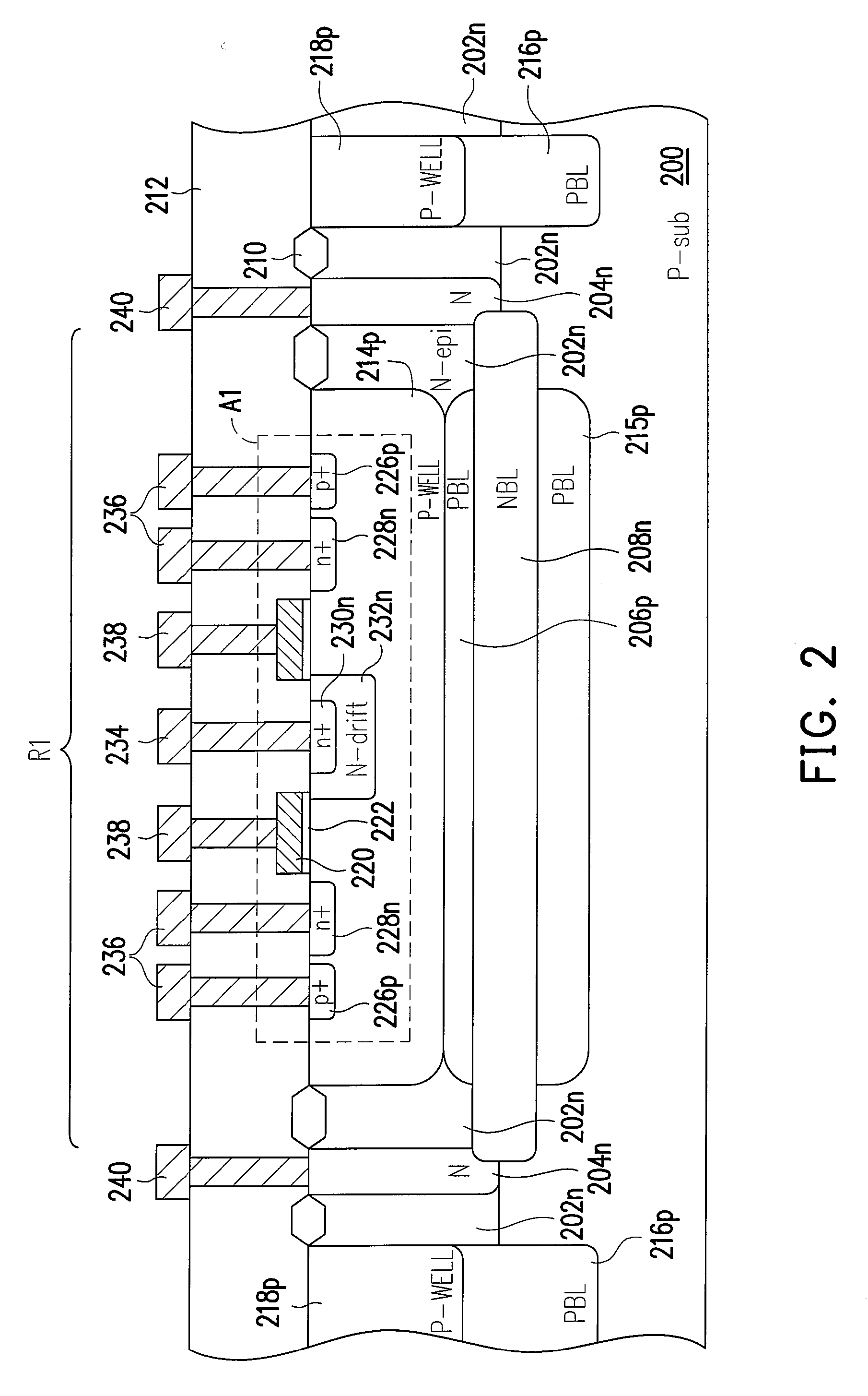
[0031]FIG. 2 is a cross-sectional view of a semiconductor device in accordance with a first embodiment of the present invention.

[0032]Referring to FIG. 2, the semiconductor device of the present invention includes a substrate 200, an epitaxial layer 202n, a sinker 204n, an active device A1, a first buried layer 206p and a second buried layer 208n. In this embodiment, the semiconductor device further includes an isolation structure 210, a dielectric layer 212, a well region 214p, a buried layer 216p, a well region 218p, interconnects 234, 236, 238 and 240, but the present invention is not limited to the particular embodiment disclosed herein. The active device A1 may be any suitable type of active devices, for example, a high voltage metal-oxide-semiconductor field effect transistor (hereinafter referred to as MOSFET) including a lateral double-diffused metal-oxide-semiconductor field effect transistors (LDMOSFET). In this embodiment, the active device A1 takes another MOSFET an exam...

second embodiment

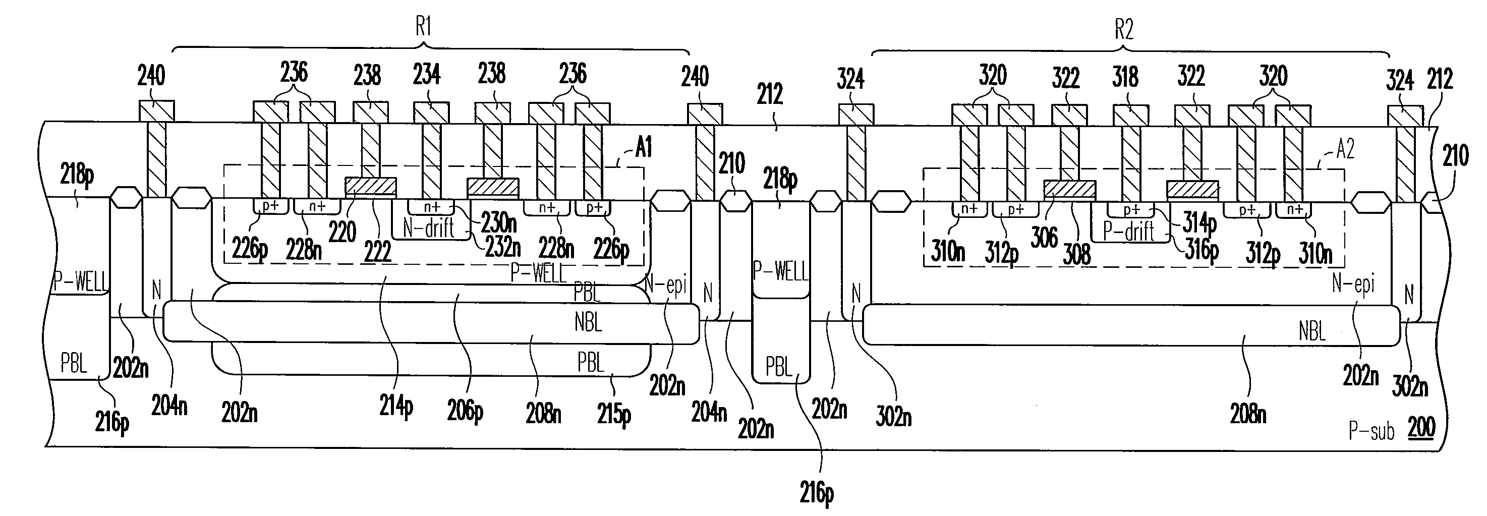
[0038]FIG. 3 is a cross-sectional view of a CMOSFET in accordance with a second embodiment of the present invention. For the sake of simplicity, only the differences between the second and first embodiments are described herein.

[0039]Referring to FIG. 3, the CMOSFET includes a first transistor and a second transistor A2. In this embodiment, the first transistor is the active device A1 as described in the first embodiment, and is, for example, a high voltage MOSFET. The second transistor A2 is, for example, also a high voltage MOSFET, but the present invention is not limited to the particular embodiment disclosed herein. In other words, the first transistor and the second transistor A2 may be any kind of MOSFET. In this embodiment, the CMOSFET further includes interconnects 318, 320, 322 and 324 formed in the dielectric layer 212, but the present invention is not limited to the particular embodiment disclosed herein.

[0040]The CMOSFET further includes a sinker 302n of the second type ...


PUM


Abstract

A semiconductor device includes a substrate, an epitaxial layer, a sinker, an active device, a first buried layer, and a second buried layer. The substrate has a first type conductivity. The epitaxial layer has a second type conductivity, and is located on the substrate. The sinker has the second type conductivity, and is located in the epitaxial layer. The sinker extends from the substrate to an upper surface of the epitaxial layer, and partitions a region off from the epitaxial layer. The active device is located within the region. The first buried layer has the first type conductivity, and is located between the region and the substrate. The second buried layer has the second type conductivity, and is located between the first buried layer and the substrate. The second buried layer connects with the sinker. Because of the above-mentioned configuration, latch-up can be prevented.

Description

BACKGROUND OF THE INVENTION[0001]1. Field of the Invention[0002]The present invention generally relates to a semiconductor device, and more particularly, to a semiconductor device which can prevent a latch-up phenomenon.[0003]2. Description of Related Art[0004]Semiconductor design must be improved along with increasing integration and increasing complicated requirements thereof. For example, the design of high voltage devices must enable the devices to operate under a high voltage without effecting operation of other devices. Restriction and problem of a high voltage device are described as follows with reference to FIG. 1.[0005]FIG. 1 is a cross-sectional view showing a conventional high voltage device. This high voltage device is a complementary metal-oxide-semiconductor field effect transistor (CMOSFET) that is composed of two lateral double-diffused metal-oxide-semiconductor field effect transistors (LDMOSFET).[0006]With reference to FIG. 1, the high voltage device comprises a P...

Claims


Application Information

Patent Timeline
Patent Type & Authority Applications(United States)
IPC IPC(8): H01L27/092
CPCH01L21/823814H01L21/823878H01L21/823892H01L29/7835H01L27/0928H01L29/1083H01L29/1087H01L27/0921
Inventor MA, SHIH-KUEILEE, CHUNG-YEHYEH, CHUN-YINGKUO, WEI-TING
Owner EPISIL TECH INC
Why Eureka
Try Eureka