Merging of infrastructure within a development environment

a technology of infrastructure and development environment, applied in the direction of cad circuit design, instrumentation, requirement analysis, etc., can solve the problem of employing comparatively tedious hardware description languages

Active Publication Date: 2005-12-15
KEYSIGHT TECH
View PDF7 Cites 30 Cited by
  • Summary
  • Abstract
  • Description
  • Claims
  • Application Information

AI Technical Summary

Problems solved by technology

However, in existing design environments, it is necessary to employ comparatively tedious hardware description languages (HDL) such as Verilog® and VHDL® in order to implement infrastructure and off-chip input-output (I / O) interfaces.

Method used


Image

  • Merging of infrastructure within a development environment
  • Merging of infrastructure within a development environment
  • Merging of infrastructure within a development environment

Examples


Embodiment Construction

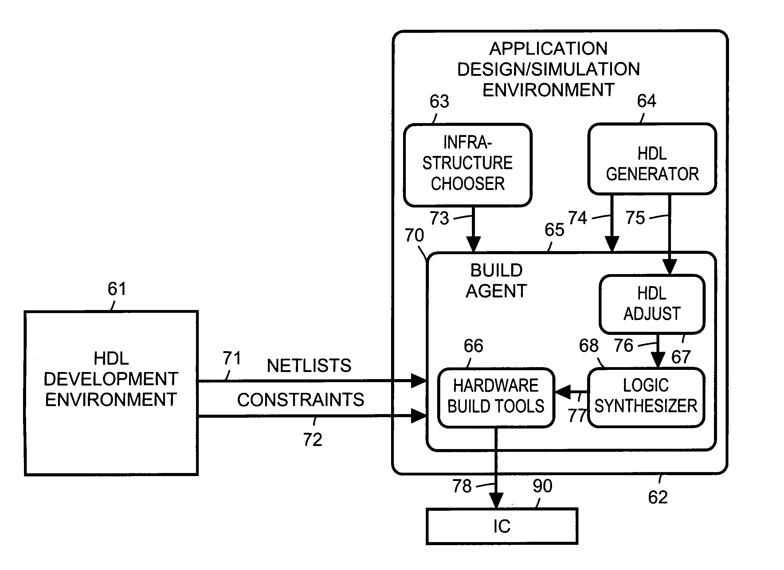
[0010]FIG. 1 is a simplified block diagram of a printed circuit board (PCB) 81. PCB 81 includes an integrated circuit (IC) 90. For example, IC 90 is a programmable logic device (PLD), such as a field-programmable gate array (FPGA).

[0011] IC 90 includes a primary logic component 98. For example, primary logic component 98 includes algorithms for digital signal processing. Alternatively primary logic component performs other functions such as complex mathematical operations associated with, for example, measurement, test, control, or communications.

[0012] IC 90 includes additional logic blocks referred to herein as support logic components (SLC). By way of illustration FIG. 1 shows seven SLCs: SLC 91, SLC 92, SLC 93, SLC 94, SLC 95, SLC 96 and SLC 97. For example, SLC 91 is an interface for IC 90 to a bus interface 82. For example, bus interface 82 is an interface to a peripheral component interconnect (PCI) bus or some other type of bus. For example, SLC 92 is an interface for IC 9...


PUM


Abstract

A development environment includes a graphical design tool and a build agent. The graphical design tool allows a designer to design a primary logic component of a circuit. The graphical design tool generates modules using a hardware description language to represent the primary logic component of the circuit. The modules include abstract references to infrastructure for the circuit. The build agent synthesizes the modules into netlists and merges the netlists with a description of the infrastructure for the circuit. The infrastructure is generated in a development environment separate from the graphical design tool. The build agent includes an adjuster that adjusts the modules. The adjustment to the modules includes replacing the abstract references to the infrastructure with actual references utilized within the infrastructure.

Description

BACKGROUND [0001] High-level, graphical design tools are often used in the design of programmable logical devices (PLDs) such as field-programmable gate arrays (FPGAs). For example, System Generator for DSP® available from Xilinx, Inc., runs within the modeling environment of Simulink® available from The MathWorks, Inc. and can be used to express, simulate and synthesize control and digital signal processing (DSP) algorithms embodied as primary logic components within field programmable gate arrays (FPGAs). However, in existing design environments, it is necessary to employ comparatively tedious hardware description languages (HDL) such as Verilog® and VHDL® in order to implement infrastructure and off-chip input-output (I / O) interfaces. This involves, for example, the detailed specification of interface circuitry, as well as the configuration of impedances, drive levels, phase delays, supply voltages and the clocking schemes and timing offsets of specialized subcircuits associated ...

Claims


Application Information

Patent Timeline
Patent Type & Authority Applications(United States)
IPC IPC(8): G06F9/44G06F9/455G06F17/50
CPCG06F17/5045G06F8/10G06F30/30
Inventor HAMILTON, ROBERT ANSONJEFFERSON, STANLEY TEDCOVERSTONE, RANDY ALLEN
Owner KEYSIGHT TECH
Why Eureka
Try Eureka