Semiconductor acceleration sensor device and method for manufacturing the same

Inactive Publication Date: 2005-12-22
LAPIS SEMICON CO LTD
View PDF15 Cites 19 Cited by
  • Summary
  • Abstract
  • Description
  • Claims
  • Application Information

AI Technical Summary

Benefits of technology

[0017] One object of the present invention is to provide a semiconductor acceleration sensor device which is low-cost and excellent for mass production while maintaining long-term reliability, and also to provide a method for manufacturing such a semicon

Problems solved by technology

Although the weight part of the acceleration sensor chip is coated with the

Method used


Image

  • Semiconductor acceleration sensor device and method for manufacturing the same
  • Semiconductor acceleration sensor device and method for manufacturing the same
  • Semiconductor acceleration sensor device and method for manufacturing the same

Examples


first embodiment

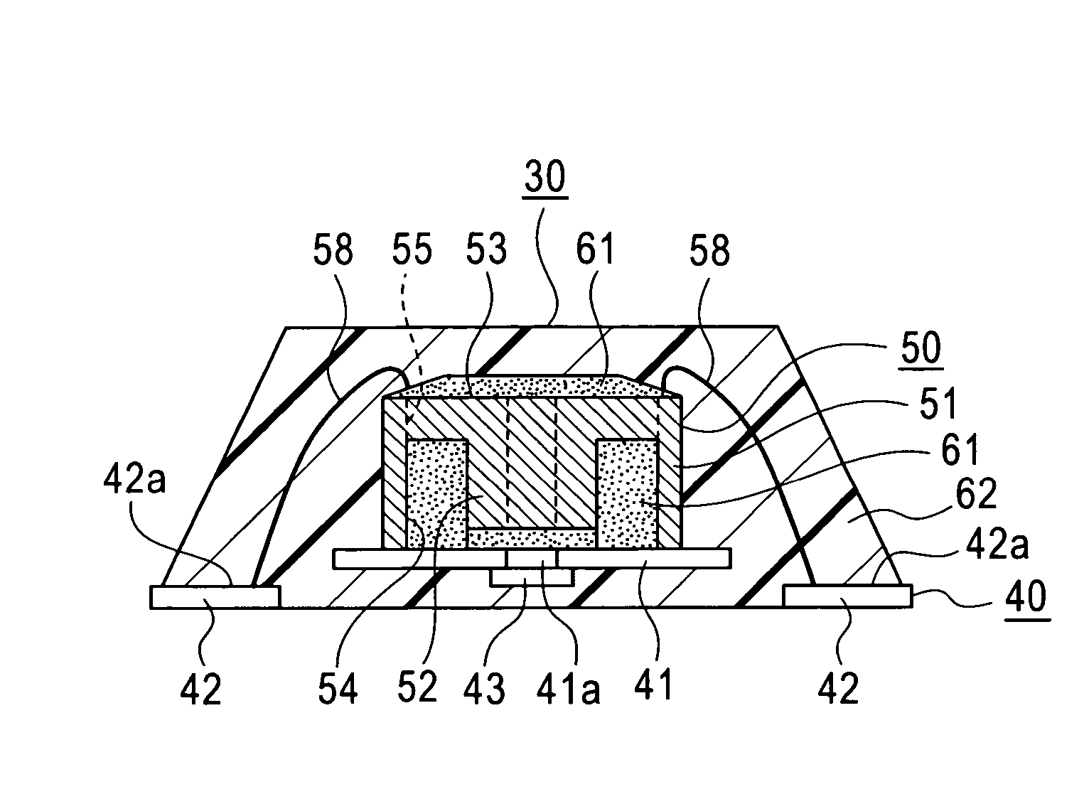
[0036] Referring to FIGS. 1A to 1F, a QFN package type semiconductor acceleration sensor device according to a first embodiment of the present invention will be described.

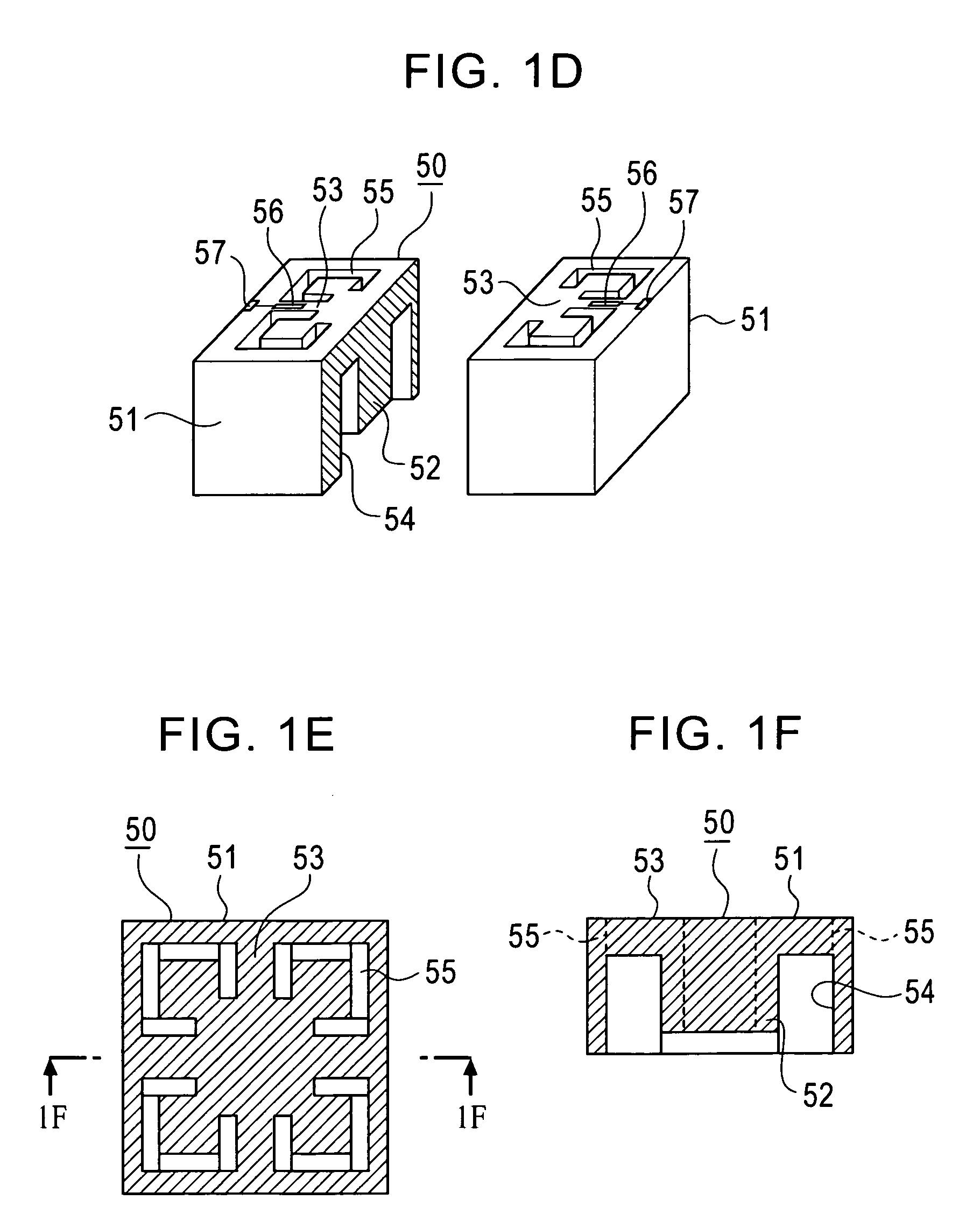
[0037] The semiconductor acceleration sensor device 30 is mounted on a lead frame 40. The lead frame 40 has a die pad 41 which is a rectangular supporting plate. In a first area of the die pad 41 which occupies the central portion of the die pad 41 is formed a first through hole 41a. Four conductive parts (for example, post sections) 42a of a plurality of leads 42 are provided around the die pad 41. On the lower surface of the die pad 41 is fixed a lid part 43 to close the through hole 41a. In a second area of the die pad 41, which surrounds the first area which occupies the central portion of the upper surface of the die pad 41 is fixed an acceleration sensor chip 50 which detects external acceleration.

[0038] The acceleration sensor chip 50 has a pedestal part (for example, a silicon chip or a semiconductor chip...

third embodiment

[0063]FIGS. 3A to 3D show another series of manufacturing steps to fabricate the semiconductor acceleration sensor device 30 shown in FIG. 1. This method is similar to that of the second embodiment. The semiconductor acceleration sensor device 30 is manufactured, for example, through the following steps (1) to (4).

[0064] (1) Step of FIG. 3A

[0065] In the same manner as shown in FIG. 2A, the acceleration sensor chip 50 is die-bonded on the die pad 41 of the lead frame 40. After the electrode pads 57 of the acceleration sensor chip 50 are bonded to the post sections 42a of the lead frame 40 by the wires 58, the lead frame 40 is turned upside down as shown in FIG. 3A.

[0066] (2) Step of FIG. 3B

[0067] The needle 63 for resin injection is positioned over the through hole 41a provided in the center of the die pad 41. Then, from the needle 63 the viscous liquid resin (for example, such as a thermosetting silicon resin) 61a is injected into the through hole 41a by only enough amount to coat...

fourth embodiment

[0075]FIG. 4 is a cross-sectional view of an SON (Small Outline Nonlead) package type semiconductor acceleration sensor device according to a fourth embodiment of the present invention. Structural elements common to those of the first embodiment shown in FIG. 1 are designated by the same or similar reference symbols.

[0076] A semiconductor acceleration sensor device 30A is mounted on a substrate (for example, a wiring board) 70. The wiring board 70 has a plurality of post sections 71 on the upper surface, and a plurality of conductive parts 72 on the lower surface. The post sections 71 and the conductive parts 72 are connected by through holes or the like which are not shown in the figure. On the post sections 71 of the wiring board 70 is flip-chip bonded an acceleration sensor chip 50 similar to that shown in FIG. 1. On a plurality of electrode pads 57 provided on the upper surface of the acceleration sensor chip 50 are respectively formed bumps 59, which are electrically connected...


PUM


Abstract

Although a weight part of an acceleration sensor chip fixed on a die pad is coated with a gelatinous resin part of low elasticity, the weight part is easily displaced by an external acceleration. Thus, an acceleration can be detected with accuracy. Furthermore, long-term reliability equal to those of regular resin packages is ensured because those portions of an acceleration sensor device which are not used for acceleration sensing are sealed with a resin part.

Description

BACKGROUND OF THE INVENTION [0001] 1. Field of the Invention [0002] This invention relates to a semiconductor acceleration sensor device utilizing a resin sealed package and a method for manufacturing the device. More particularly, this invention relates to the device utilizing an MEMS (Micro Electro Mechanical Systems) or an MCP (Multi Chip Package). The MCP is a package on which an MEMS and a semiconductor circuit chip are mounted together. [0003] 2. Description of the Related Art [0004] In recent years, with reduced sizes and thicknesses of electronic devices, attention is focused on an MEMS technology, which enables fabrication of sensors or electromechanical parts or the like in a micrometer size. [0005]FIGS. 8A to 8C of attached drawings show cross-sectional views of examples of the constitution of semiconductor acceleration sensor devices utilizing a conventional MEMS package. FIG. 8A illustrates a single-chip type device, FIG. 8B a multi-chip type (a stacked type) device, an...

Claims


Application Information

Patent Timeline
IPC IPC(8): G01P15/08B81B7/02G01P1/02G01P15/12H01L21/56H01L23/28
CPCG01P1/023G01P15/123G01P15/18H01L2224/48091H01L2224/48137H01L2224/48247H01L2924/1461H01L2924/10253H01L2924/00014H01L2924/00H01L24/97G01P2015/0842A47J37/0676A47J37/0786A23L5/30
Inventor SHIZUNO, YOSHINORI
Owner LAPIS SEMICON CO LTD
Why Eureka
Try Eureka