

MIM capacitors
a technology of metal-insulator metal and capacitor, which is applied in the direction of capacitors, semiconductor devices, electrical devices, etc., can solve the problems of limited area capacitance, restriction in the selection of mim dielectric materials, and alignment problems to underlying features, so as to reduce lithography steps, increase area capacitance, and reduce cost
- Summary
- Abstract
- Description
- Claims
- Application Information
AI Technical Summary
Benefits of technology
Problems solved by technology
Method used
Image

Examples
Embodiment Construction
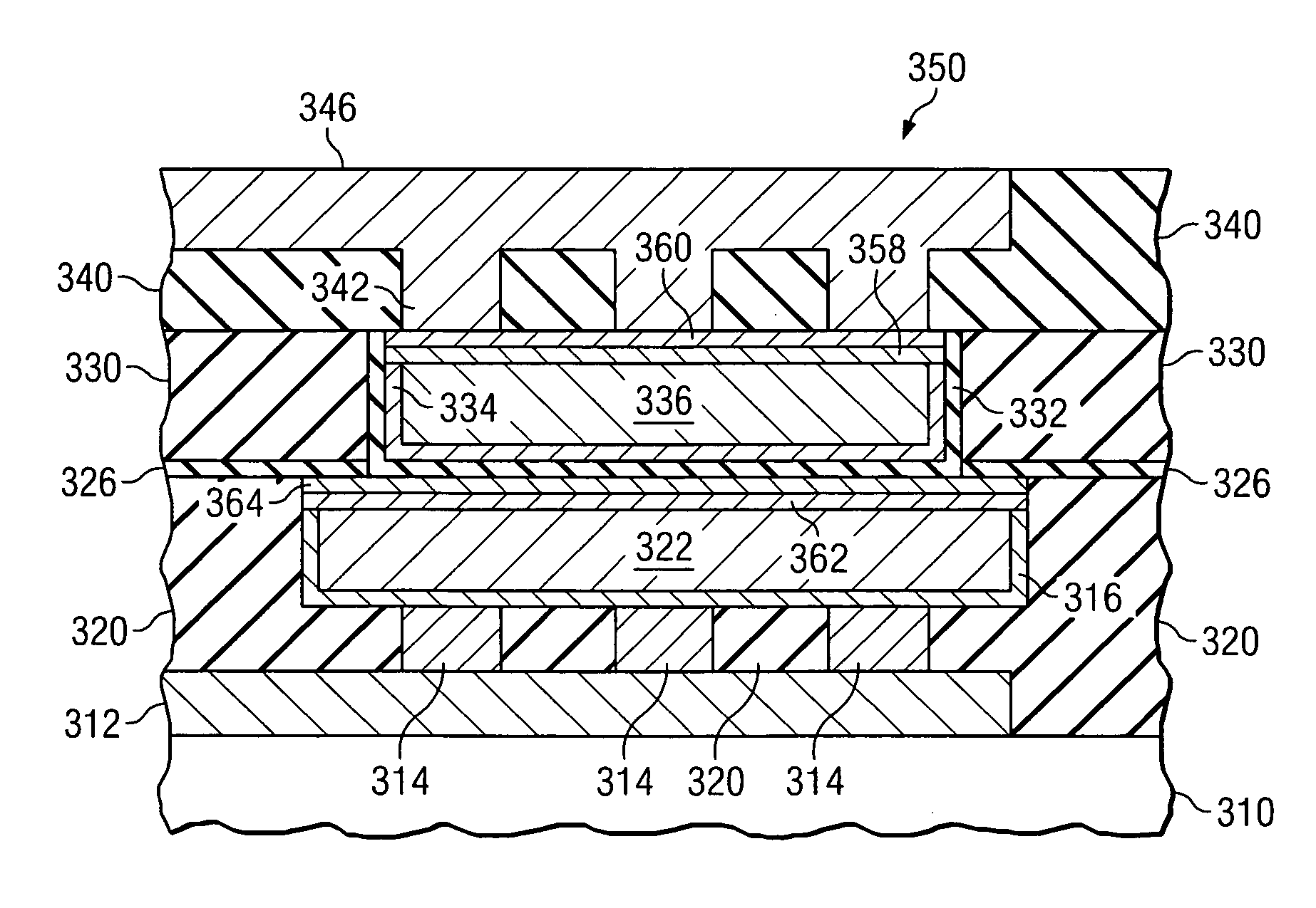
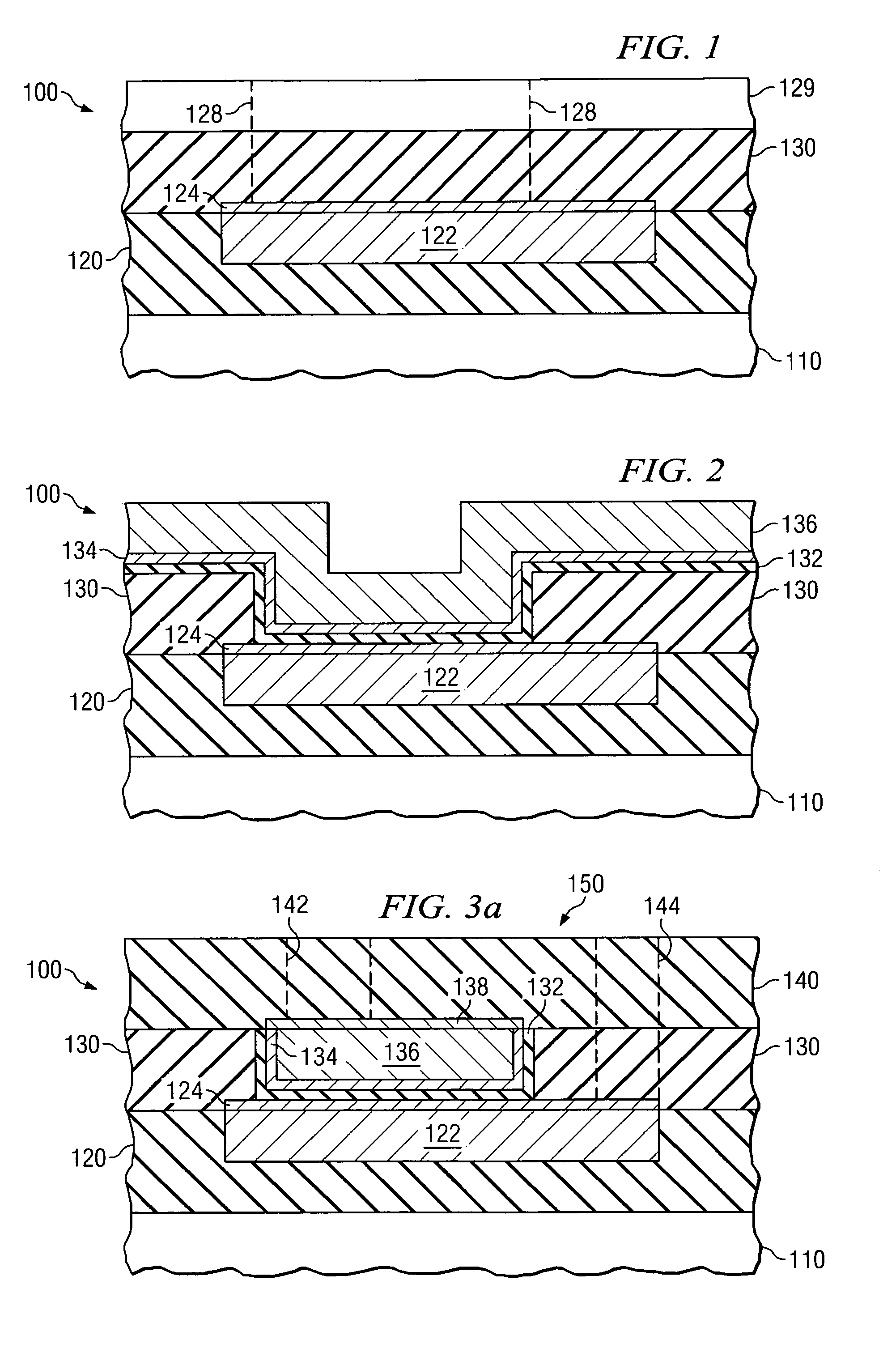
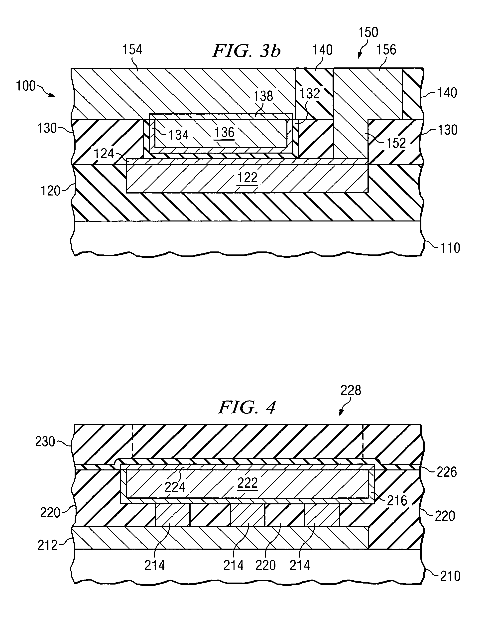
[0022] The making and using of the presently preferred embodiments are discussed in detail below. It should be appreciated, however, that the present invention provides many applicable inventive concepts that can be embodied in a wide variety of specific contexts. The specific embodiments discussed are merely illustrative of specific ways to make and use the invention, and do not limit the scope of the invention. Only one MIM capacitor is shown in each figure, although many MIM capacitors, other components and / or conductive lines may be present within each layer.
[0023] With reference now to FIG. 1, therein is shown a semiconductor wafer 100 having a substrate 110. The substrate 110 typically comprises a semiconductor material such as single-crystal silicon, and may include other conductive layers or other semiconductor elements such as transistors or diodes, as examples (not shown). The substrate 110 may alternatively comprise compound semiconductors such as GaAs, InP, Si / Ge, SiC, ...
PUM
 Abstract
Description
Claims
Application Information