Stacked semiconductor memory device

a memory device and semiconductor technology, applied in semiconductor devices, instruments, electrical appliances, etc., can solve the problems of increasing the cost of developing a wide variety of memory devices with each year, limiting the miniaturization of semiconductors, and not making a disclosure regarding the number of input/output bits and the number, etc., to achieve the effect of reducing the cost of developing a wide variety of memory devices

Active Publication Date: 2005-12-29
NEC CORP +1
View PDF4 Cites 98 Cited by
  • Summary
  • Abstract
  • Description
  • Claims
  • Application Information

AI Technical Summary

Benefits of technology

[0018] According to the present invention, in a memory device in which memory cell array chips and interface chips are stacked, the input / output bit configuration of the memory cell array chips and the data transfer rate are changed by the memory configuration switching circuits of the interface chips. In this way, the cost of developing a wide variety of memory devices can be reduced.

Problems solved by technology

However, the miniaturization of semiconductors has limits, and there is consequently a need for the introduction of new techniques for achieving greater increases in capacity.
However, although each of the above-described multilayered memory devices enables an increase in memory capacity within a limited chip area, no disclosure is made regarding the number of input / output bits and the number of banks, which are constituent elements of the memory, or regarding the data transfer rate.
The diversification of systems has resulted in a wide variety of memory configurations, and as a result, many varieties of memory devices must be developed, and the cost of developing these memory devices grows with each year.

Method used


Image

  • Stacked semiconductor memory device
  • Stacked semiconductor memory device
  • Stacked semiconductor memory device

Examples


Embodiment Construction

[0047] Explanation next regards working examples of the present invention with reference to the accompanying figures.

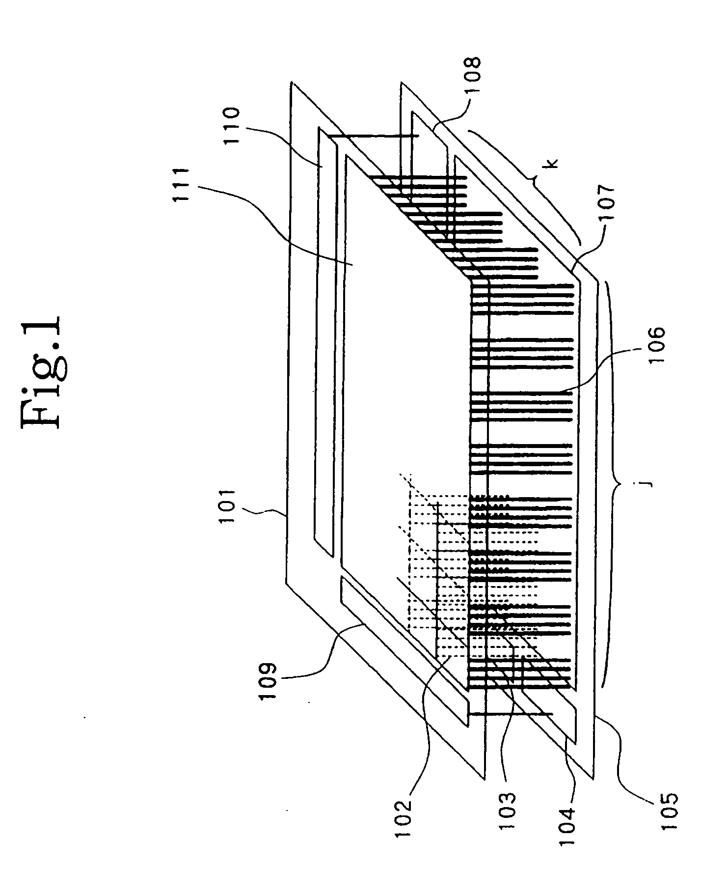
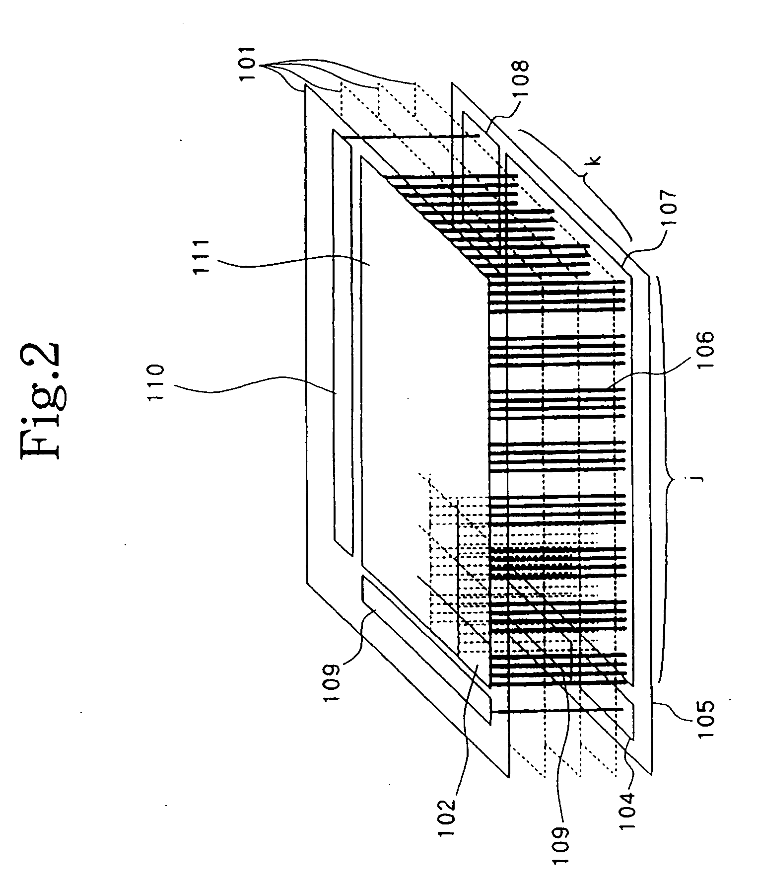
[0048]FIG. 1 is a schematic view of the configuration of a working example of the stacked memory device according to the present invention.

[0049] As shown in FIG. 1, the present working example is made up of: memory cell array chip 101, memory unit 102, input / output buffer 103, address buffer 104, interface chip 105, interchip wires 106, memory configuration switching circuit 107, address buffer 108, row decoder 109, column decoder 110, and memory cell array 111.

[0050] Memory cell array 111 is made up from a plurality of memory units 102 that are arranged in a matrix; this matrix being integrated with row decoder 109 and column decoder 110 to make up memory cell array chip 101. Interface chip 105 is made up of address buffer 104, input / output buffer 103, and memory configuration switching circuit 107; is stacked with memory cell array chip 101; and is connected to ...


PUM


Abstract

The stacked semiconductor memory device of the present invention has the object of reducing the cost of developing a wide variety of memory devices and includes: a memory cell array chip that is equipped with memory cell arrays, an interface chip that is stacked with the memory cell array chip and that is provided with a memory configuration switching circuit for changing the input/output bit configuration of the memory cell arrays, and a plurality of interchip wires for connecting the memory cell array chip and the interface chip.

Description

BACKGROUND OF THE INVENTION [0001] 1. Field of the Invention [0002] The present invention relates to a semiconductor memory device, and more particularly to a semiconductor memory device in which a memory cell array chip and an interface chip for changing the memory configuration are stacked. [0003] 2. Description of the Related Art [0004] With the miniaturization and increased integration of semiconductor integrated circuits, DRAM (Dynamic Random Access Memory) and SRAM (Static Random Access Memory) have achieved memory having greatly increased capacity. However, the miniaturization of semiconductors has limits, and there is consequently a need for the introduction of new techniques for achieving greater increases in capacity. [0005] A three-dimensional semiconductor in which semiconductor chips are stacked has been proposed as one technique for achieving greater capacity. Japanese Patent Laid-Open Publication No. H04-196263 discloses the realization of a large-scale integrated cir...

Claims


Application Information

Patent Timeline
Patent Type & Authority Applications(United States)
IPC IPC(8): G11C5/02G11C5/06H01L21/20H01L27/108H01L29/76H01L29/94H01L31/119
CPCG11C5/02G11C5/063G11C5/025
Inventor SAITO, HIDEAKIHAGIHARA, YASUHIKOFUKAISHI, MUNEOMIZUNO, MASAYUKIIKEDA, HIROAKISHIBATA, KAYOKO
Owner NEC CORP
Why Eureka
Try Eureka