Spread spectrum clock generation circuit, jitter generation circuit and semiconductor device

a clock generation circuit and jitter generation technology, applied in oscillation comparator circuits, automatic control of pulses, instruments, etc., can solve the problems of increased electromagnetic wave radiation at this part, increased cost, and inability to secure normal operation, so as to reduce radiation noise and reduce the effect of operation speed and radiation nois

Active Publication Date: 2005-12-29
MONTEREY RES LLC
View PDF20 Cites 16 Cited by
  • Summary
  • Abstract
  • Description
  • Claims
  • Application Information

AI Technical Summary

Benefits of technology

[0012] However, it is not easy to generate such a waveform as shown in FIG. 3, and the scale of a circuit which generates such a waveform becomes larger, resulting in a problem of higher cost.
[0052] Moreover, when the internal circuit in the semiconductor device can be classified into a plurality of groups whose operation frequency is different, a plurality of jitter generation circuits which add a different amount of jitter are provided to supply a jitter to each circuit group in accordance with the operation frequency. It is also possible to supply a clock signal, to which a jitter is not added, to a circuit group whose operation timing is strict and whose operation frequency is high. In this manner, as it is possible to adjust the amount of jitter in accordance with the operation frequency, the speed of the circuit operation can be increased and at the same time the radiation noise can be reduced. In this case, the jitter generation circuit can be one according to the fifth aspect of the present invention or to another one.

Problems solved by technology

When a triangular wave is used, however, as peaks occur at both ends of the width of the spectrum generated by the spread, a problem occurs that the electromagnetic wave radiation at this part is increased.
However, it is not easy to generate such a waveform as shown in FIG. 3, and the scale of a circuit which generates such a waveform becomes larger, resulting in a problem of higher cost.
This is undesirable from the standpoint of the operation of an SSCG circuit.
When a generated clock is used in a logic circuit or the like, there is no operational problem if the rate of change with respect to time is small even though the range of change is large, but if the period suddenly changes considerably, a problem occurs that a normal operation is not secured.
Therefore, when this clock pulse generator is used, a problem occurs that it is not possible to add a proper jitter in accordance with the frequency, if the clock frequency is changed.
In addition to the delay circuit, a multiplexer and a circuit to control the multiplexer are required for the clock pulse generator, therefore a problem occurs that the circuit configuration becomes more complex.

Method used


Image

  • Spread spectrum clock generation circuit, jitter generation circuit and semiconductor device
  • Spread spectrum clock generation circuit, jitter generation circuit and semiconductor device
  • Spread spectrum clock generation circuit, jitter generation circuit and semiconductor device

Examples


first embodiment

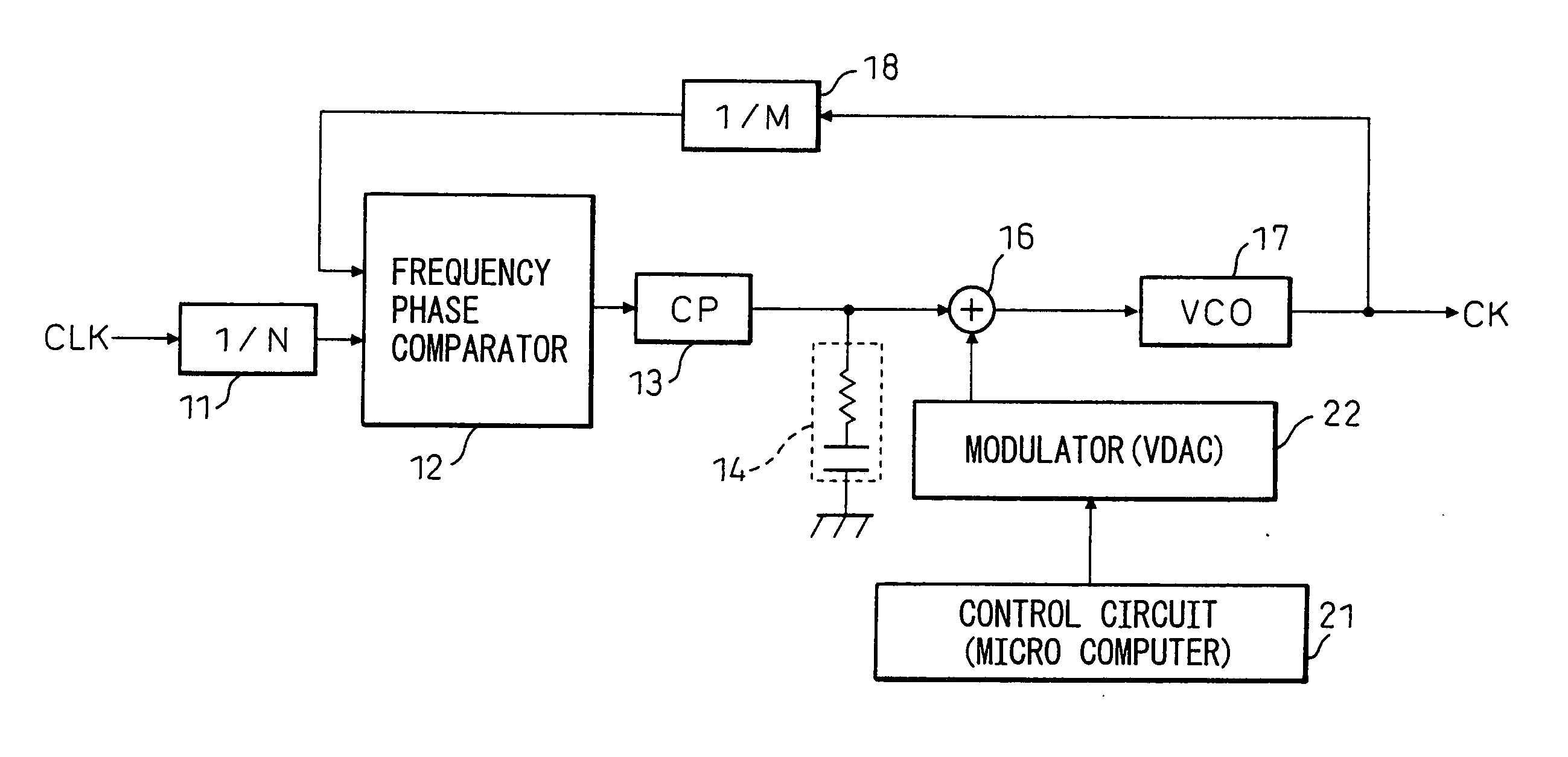
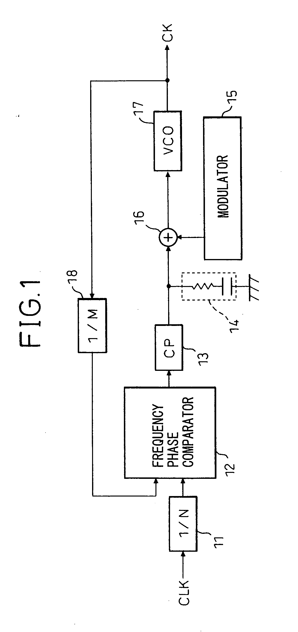
[0125]FIG. 8 is a diagram showing the configuration of the spread spectrum clock generation (SSCG) circuit in the present invention. As shown schematically, this circuit is a circuit in which a clock CK M / N times the reference clock CLK is generated therefrom by the use of a PLL circuit as in the circuit shown in FIG. 1 but differs from a conventional one in that the period of a spread spectrum modulation signal generated by a modulator 22 changes in order as shown in FIG. 5A.

[0126] As shown in FIG. 8, in the SSCG circuit in the first embodiment, a control circuit 21 generates an output code such as shown in FIG. 9 and outputs it to the modulator 22. The modulator 22 is a voltage digital-to-analog converter (VDAC) and converts the output code into an analog voltage signal. In this manner, a spread spectrum modulation analog voltage signal as shown in FIG. 5A is obtained. When the voltage signal does not change smoothly because of the voltage change width corresponding to the least s...

fifth embodiment

[0148] In the SSCG circuit in the fifth embodiment, the control circuit 21 generates an output code as shown in FIG. 24 and outputs it to the modulator 22. In the first period, the value of this output code increases from the middle value to the first maximum value and decreases to the first minimum value, and then increases again. The period enters the second period when the middle value is reached, and after the value increases from the middle value to the second maximum value, it decreases to the second minimum value, and then increases again. When the middle value is reached, the period enters the first period again, and the same operation is repeated. In this example, the length of one period of the first period is different from that of the second period. If the voltage signal does not change smoothly because of the voltage change width corresponding to the least significant bit of the output code, a low-pass filter is used for smoothing. In this manner, the voltage to be appl...

second embodiment

[0154] In this manner, the spread spectrum voltage signal whose amplitude changes for each period is obtained. In the second embodiment also, both the amplitude and the period of the spread spectrum voltage signal change. In order to generate a spread spectrum voltage signal only the amplitude of which changes and the period of which does not change, a constant current source capable of charging or discharging with different currents is provided in the circuit shown in FIG. 26A and the current to be supplied is switched for each period. In this case, the switch control circuit 35 switches the power supply between charging and discharging in a predetermined period.

[0155] Further, the spread spectrum modulation signal shown in FIG. 67 can be also obtained in the above circuit. In this case, the current to be supplied is switched in each cycle.

[0156] Although a case of switching between two amplitudes is shown here, it is also possible to switch among three or more amplitudes.

[0157] ...


PUM


Abstract

A spread spectrum clock generation circuit capable of further reducing the electromagnetic wave radiation with a simple configuration has been disclosed and, particularly in a spread spectrum clock generation circuit using a current control oscillator (ICO), a differential signal to which a spread spectrum modulation signal, the period or amplitude of which changes, is added is generated, and the differential signal is applied to the ICO and a clock is generated.

Description

BACKGROUND OF THE INVENTION [0001] The present invention relates to a spread spectrum clock generation circuit which generates a clock signal the period of which changes slightly in order to reduce electromagnetic wave radiation, a jitter generation circuit which adds a jitter to a clock signal or the like, and a semiconductor device using the circuits. [0002] Recently, as semiconductor devices have increased in speed and degree of integration, a problem of EMI (electromagnetic interference) due to electromagnetic wave radiation from a device has attracted more attention. As the operation frequency has increased, the wavelength has become shorter and shorter, and the wiring length of a connecting circuit, or inside the substrate, has become almost as short as the wavelength of a high frequency signal, therefore, the connecting sections of wires or the like may serve as antennas and electromagnetic wave radiation is increased. The electromagnetic wave radiation of electronic devices ...

Claims


Application Information

Patent Timeline
Patent Type & Authority Applications(United States)
IPC IPC(8): H03L7/00H03L7/08H03L7/089H03L7/099H03L7/18H03M1/06H03M1/08H03M1/74H04B15/02
CPCH03C3/095H03D13/004H03L7/08H03L7/0891H03L7/18H03L7/093H03L7/099H03L7/0995H03L7/0895H03L7/00
Inventor MIYATA, SHINJIOKADA, KOUJIIIJIMA, MASAOSAITOU, TERUHIKOMIYAZAKI, YUKISATO
Owner MONTEREY RES LLC
Why Eureka
Try Eureka