Fixed network resistor

a technology of fixed network resistor and resistor shell, which is applied in the direction of resistor details, resistor housing/enclosement/embedding, resistor details, etc., can solve the problems of reducing the strength of these areas, and affecting the quality of the final produ

Active Publication Date: 2005-12-29
ROHM CO LTD
View PDF6 Cites 9 Cited by
  • Summary
  • Abstract
  • Description
  • Claims
  • Application Information

AI Technical Summary

Benefits of technology

[0017] During the soldering of fixed resistor networks, to eliminate solder bridging between neighboring terminal electrodes across an intervening recess, the width of the recess between the terminal electrodes should be made larger than the width of the terminal-electrode-forming areas of the insulating substrate.
[0018] However, making the width of the recesses larger than the width of the terminal-electrode-forming areas without increasing the pitch of the terminal electrodes means that the width of the terminal-electrode-forming areas will be smaller, reducing the strength of these areas and leading to a higher occurrence of defects such as the chipping or breaking off of material.
[0020] That is, by having the width of the terminal-electrode-forming areas between the recesses and the width of the recesses satisfy the above conditions, the chipping or breaking off of material at the terminal-electrode-forming areas can be reliably prevented without increasing the pitch of the film resistors, and thus without making the insulating substrate larger. At the same time, during soldering, solder bridging between neighboring terminal electrodes across an intervening recess can be greatly reduced.
[0022] In this arrangement, when the pitch between the terminal electrodes is 0.4 mm, the width of the recesses along the lengthwise sidewalls of the insulating substrate becomes 0.21 to 0.25 mm, and the width of the terminal-electrode-forming areas between the recesses along the lengthwise sidewalls of the insulating substrate becomes 0.19 to 0.15 mm. As illustrated in detail below in the following embodiments, this has the effect of making it possible to satisfy at the same time conditions (a), (b) and (c) required of fixed resistor networks.
[0023] Moreover, in this second aspect of the invention, as noted above, in addition to making the width of the recesses along the lengthwise sidewall of the insulating substrate from 0.525 to 0.625 times the pitch of the terminal electrodes and making the width of the terminal-electrode-forming areas between the recesses along the lengthwise sidewall of the insulating substrate from 0.475 to 0.375 times the pitch of the terminal electrodes, by also setting the depth of the recesses from the lengthwise sidewall of the insulating substrate to from 0.512 to 0.645 times the width of the terminal-electrode-forming areas, the depth of the recesses from the lengthwise sidewall of the insulating substrate becomes 0.077 to 0.12 mm. This has the effect of, in addition to above conditions (a), (b) and (c), also satisfying at the same time above condition (d).

Problems solved by technology

However, making the width of the recesses larger than the width of the terminal-electrode-forming areas without increasing the pitch of the terminal electrodes means that the width of the terminal-electrode-forming areas will be smaller, reducing the strength of these areas and leading to a higher occurrence of defects such as the chipping or breaking off of material.

Method used


Image

  • Fixed network resistor
  • Fixed network resistor
  • Fixed network resistor

Examples


first embodiment

[0039] FIGS. 1 to 4 show the invention.

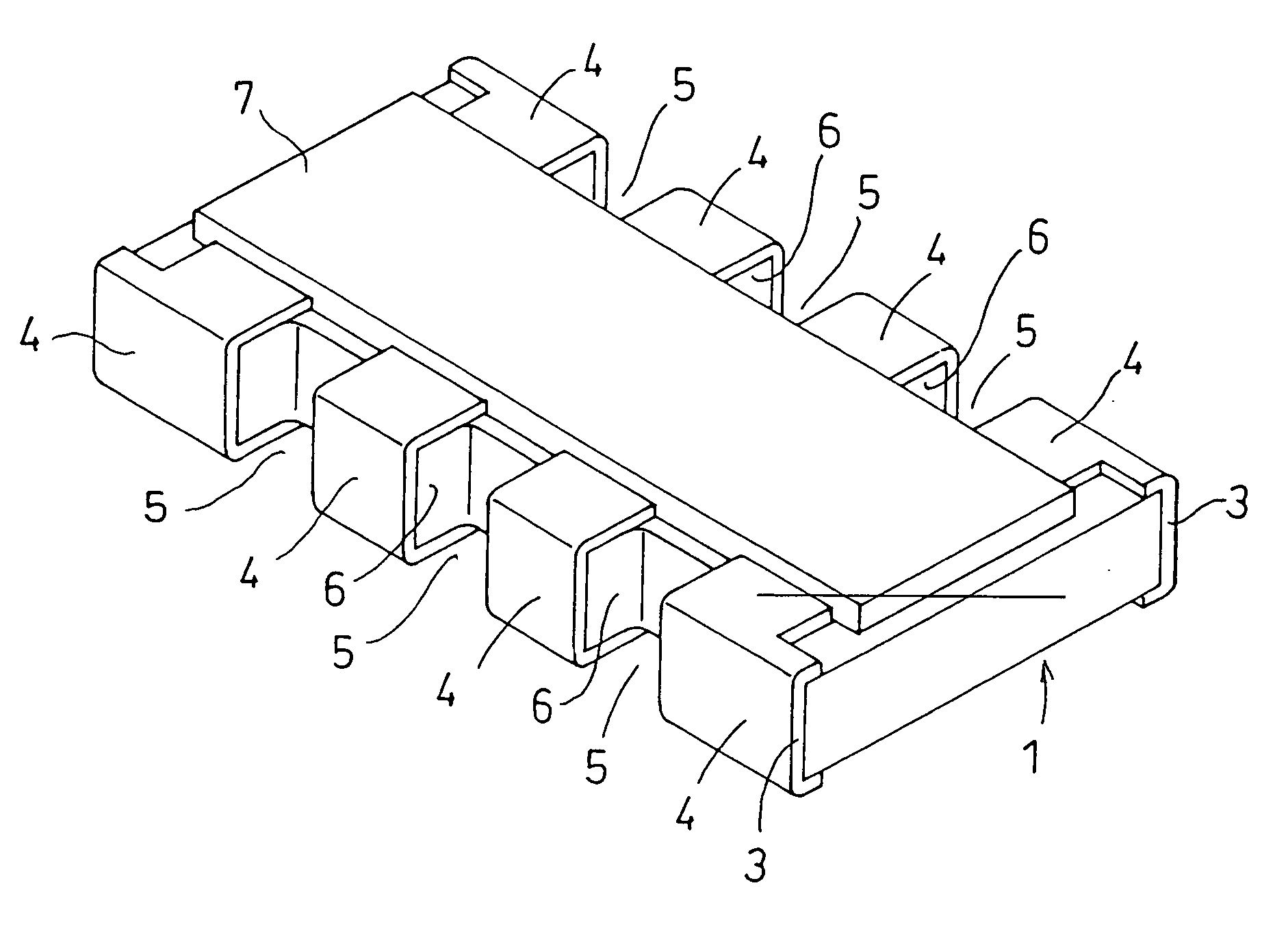
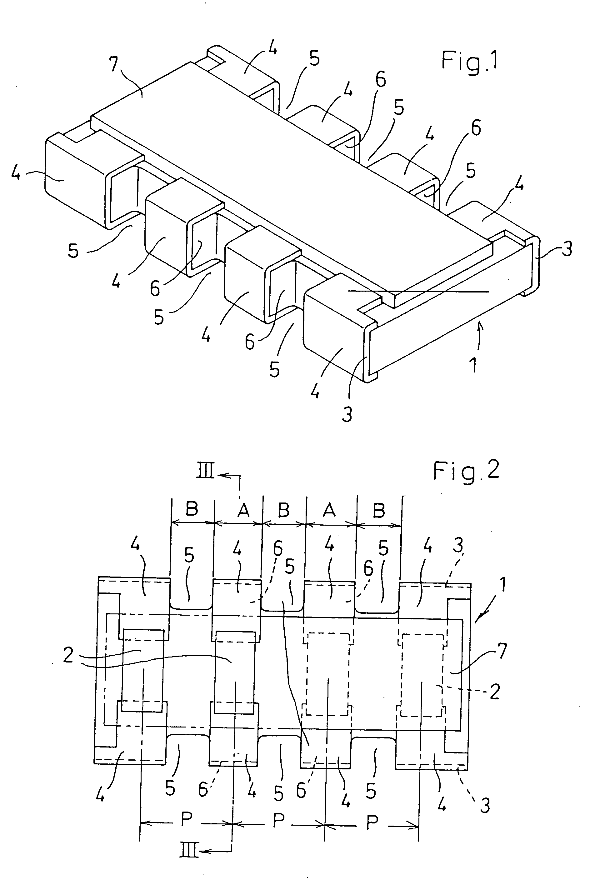
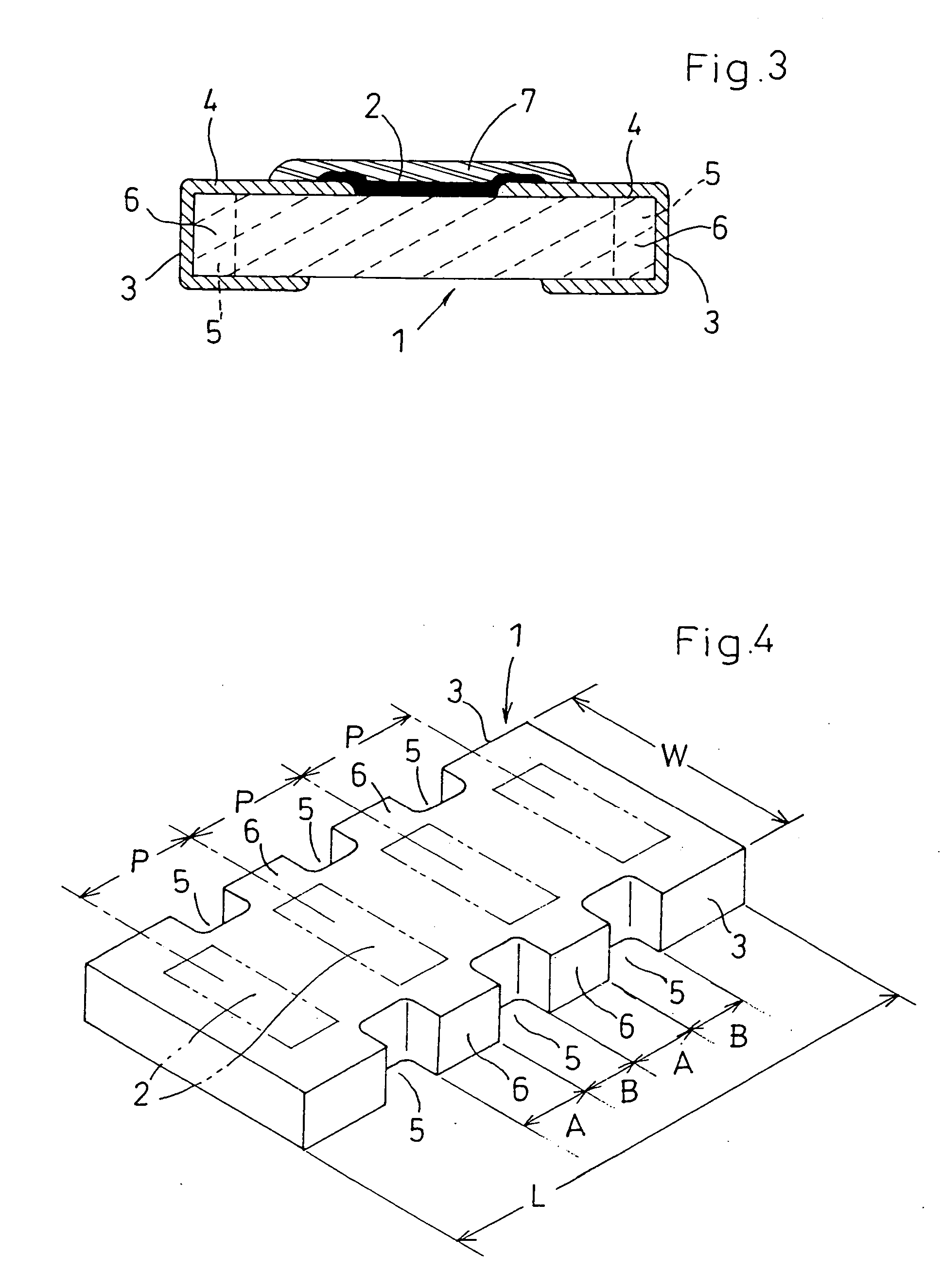
[0040] In these diagrams, the symbol 1 represents a ceramic insulating substrate having, in a plan view, a rectangular shape with a length L of 2.0 mm and a width W of 1.0 mm. This insulating substrate 1 has formed, on a top surface thereof, four film resistors 2 which are arranged in the lengthwise direction of the insulating substrate 1.

[0041] Terminal electrodes 4 which are electrically connected to both ends of each film resistor 2 are formed on both longitudinal sidewalls 3 of the insulating substrate 1 at a pitch P=0.5 mm along the longitudinal sidewalls 3. Recesses 5 are provided in areas between the individual terminal electrodes 4 on both of the lengthwise sidewalls 3 of the insulating substrate 1.

[0042] Each terminal electrode 4 is formed so as to extend to a bottom surface of the insulating substrate 1. On the top surface of the insulating substrate 1, a cover coat 7 made of a material such as glass is formed so as to cover each fi...

second embodiment

[0047] Next, FIGS. 5 and 6 show the invention.

[0048] This second embodiment is a three-element fixed resistor network composed of a single insulating substrate 11, of rectangular shape in a plan view, on which three film resistors 12 are arranged. Terminal electrodes 14 for both ends of the individual film resistors 12 are formed on both lengthwise sidewalls 13 of the insulating substrate 11 at a pitch P=0.5 mm along the lengthwise sidewalls 3, and recesses 15 are provided between the terminal electrodes 14. In addition, a cover coat 17 is formed on a top surface of the insulating substrate 11.

[0049] In this embodiment as well, by setting the terminal-electrode-forming areas 16 between the recesses 15 to a width A along the lengthwise sidewalls 13 such that A=(0.52 to 0.56)×P and setting the recesses 15 to a width B along the lengthwise sidewalls 13 such that B=(0.48 to 0.44)×P, defects such as the chipping or breaking off of material in the terminal-electrode-forming areas 16 can ...

fifth embodiment

[0058] FIGS. 9 to 11 show the invention.

[0059] This embodiment is a four-element fixed resistor network in which the pitch P between the terminal electrodes was set at 0.4 mm.

[0060] In these diagrams, the symbol 41 represents a ceramic insulating substrate having, in a plan view, a rectangular shape with a length L of 1.39 mm and a width W of 0.6 mm. This insulating substrate 41 has formed, on a top surface thereof, four film resistors 42 so as to be arranged in the lengthwise direction of the insulating substrate 41.

[0061] Terminal electrodes 44 that are electrically connected to both ends of the film resistors 42 are formed, on lengthwise sidewalls 43 at both edges of the insulating substrate 41, at a pitch P=0.4 mm along the lengthwise direction of the insulating substrate 41.

[0062] Recesses 45 having a width B along the lengthwise sidewall 43 and a suitable depth C from the lengthwise sidewall 43 are provided in areas between the terminal electrodes 44 on the lengthwise sidew...


PUM


Abstract

A fixed resistor network has an insulating substrate, a plurality of film resistors arranged on a top surface of the insulating substrate, terminal electrodes formed for the film resistors on each lengthwise sidewall of the insulating substrate at a given pitch along the sidewall, and recesses provided between the terminal electrodes. The occurrence of solder bridges between the terminal electrodes during solder mounting and the occurrence of chipping in the terminal-electrode-forming areas between the recesses on the lengthwise sidewall are both reduced by making the width of the recesses along the lengthwise sidewall either 0.44 to 0.48 times or 0.525 to 0.625 times the pitch.

Description

TECHNICAL FIELD [0001] The present invention relates to a surface-mount fixed network resistor having a single insulating substrate of rectangular shape on a top surface of which are arranged at least three film resistors, and on a lengthwise side of which are formed terminal electrodes for solder connection for each of the resistor films. BACKGROUND ART [0002] In a prior-art fixed resistor network of this type having, for example, four film resistors such as that shown in FIGS. 12 to 14, an insulating substrate 1′ with a rectangular shape of length L and width W as seen in plan view has four film resistors 2′ arranged on a top surface of the substrate 1′ in the lengthwise direction thereof and has, for both ends of each film resistor 2′, terminal electrodes 4′ which are formed on both lengthwise sidewalls 3′ of the insulating substrate 1′. The fixed resistor network is surface mounted on a printed board by soldering each of the terminal electrodes 4′. [0003] In addition, the prior ...

Claims


Application Information

Patent Timeline
Patent Type & Authority Applications(United States)
IPC IPC(8): H01C1/16H01C13/02H05K3/34
CPCH01C1/16H01C13/02H05K2201/10045H05K2201/09172H05K3/3442Y02P70/50
Inventor KURIYAMA, TAKAHIRO
Owner ROHM CO LTD
Why Eureka
Try Eureka