

Transistor performance analysis system
a technology of performance analysis and transistor, applied in the field of semiconductor production, can solve the problems of difficult to effectively difficult to analyze the large volume of data, and prone to large variations in data collected
- Summary
- Abstract
- Description
- Claims
- Application Information
AI Technical Summary
Problems solved by technology
Method used
Image

Examples
Embodiment Construction
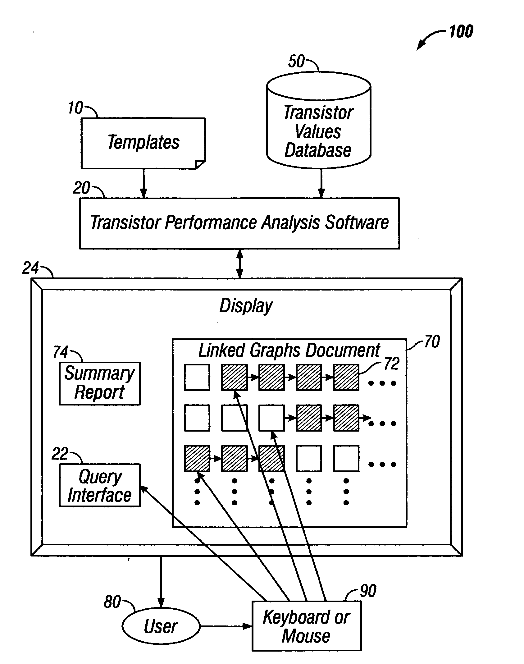
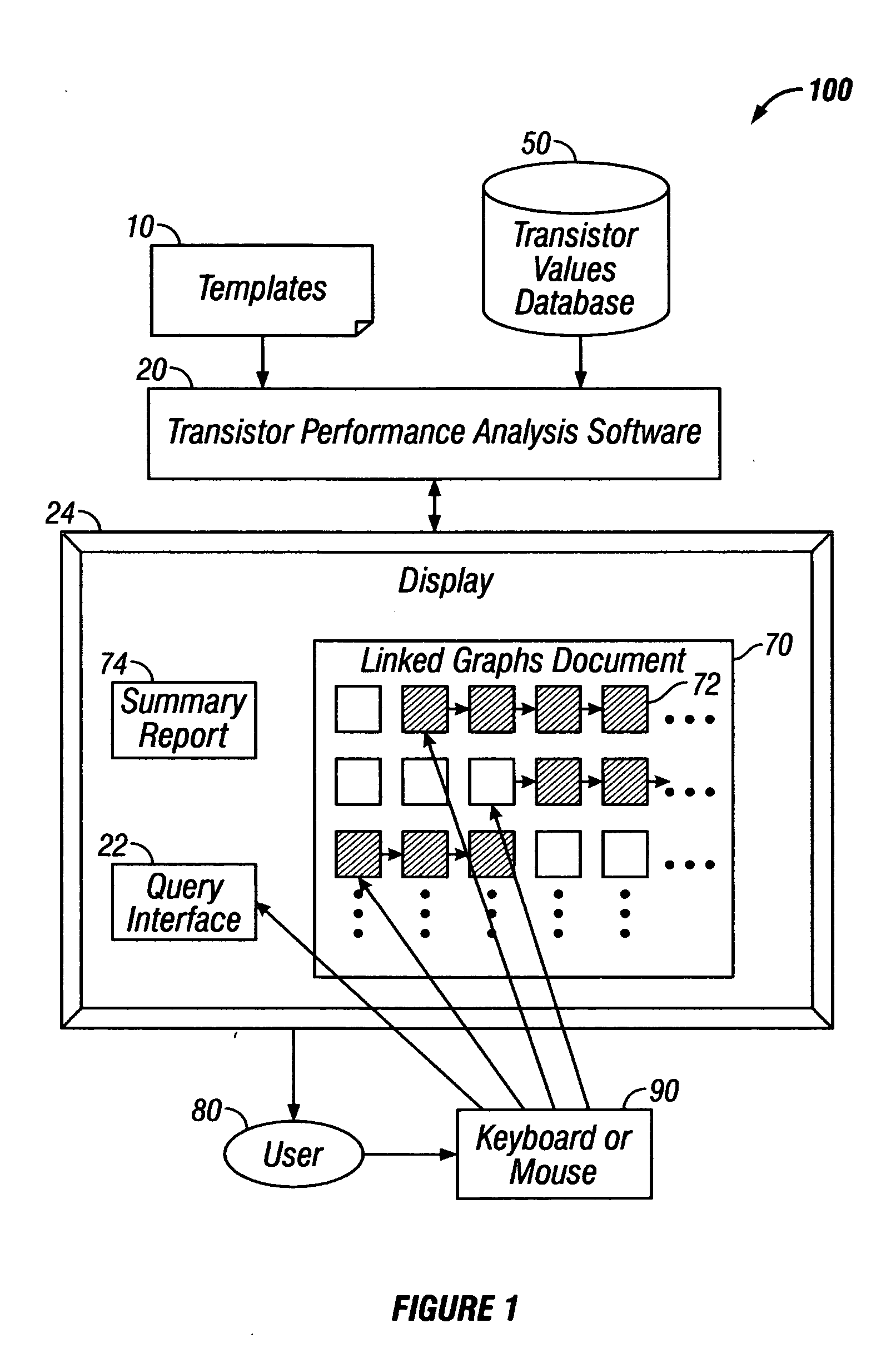
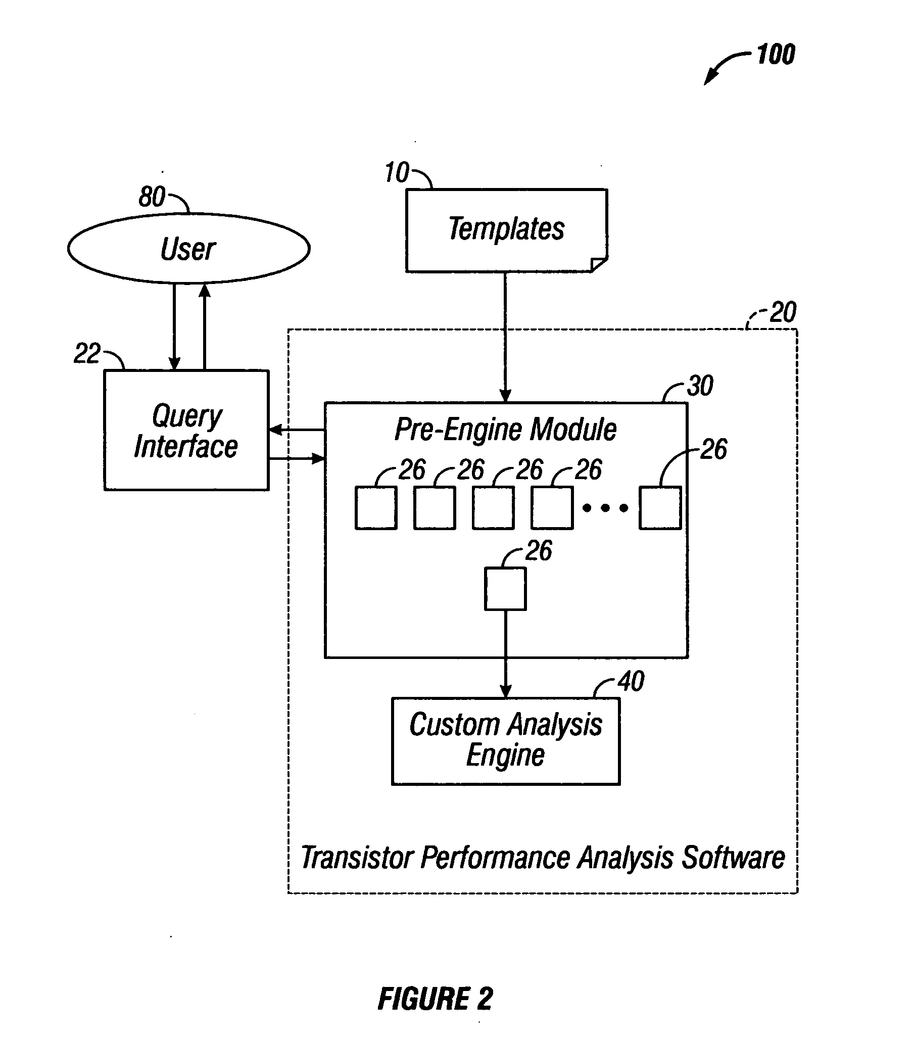
[0026] In accordance with the embodiments described herein, a system is disclosed for efficiently and automatically conducting transistor performance analysis. The system includes a transistor performance analysis software program, which takes as inputs a specification from the user of an analysis template and the material to be analyzed. The analysis template describes the parameters to be extracted and the analyses to be performed. The software extracts the values of the parameters obtained during testing of the transistors, and produces an output document with linked graphs that is suitable for performing interactive analysis, as well as a summary document following the analysis.
[0027] The transistor performance analysis software produces hundreds of linked, interactive graphs based on the chosen template, which specifies parameters, charting options, and algorithms used to generate the graphs. In some embodiments, 500 sets of data, including 500 graphs, are generated from 100,0...
PUM
 Abstract
Description
Claims
Application Information