
Semiconductor chip package with thermoelectric cooler

a technology of thermoelectric cooler and semiconductor chip, which is applied in the direction of semiconductor device details, semiconductor/solid-state device details, electrical apparatus, etc., can solve the problems of difficult to realize the release of heat between the chips, increase the amount of heat generation, and the semiconductor chip package, so as to improve thermal performance, increase operating speed, and enhance thermal performance

Active Publication Date: 2006-01-05
SAMSUNG ELECTRONICS CO LTD
View PDF6 Cites 26 Cited by
  • Summary
  • Abstract
  • Description
  • Claims
  • Application Information

AI Technical Summary

Benefits of technology

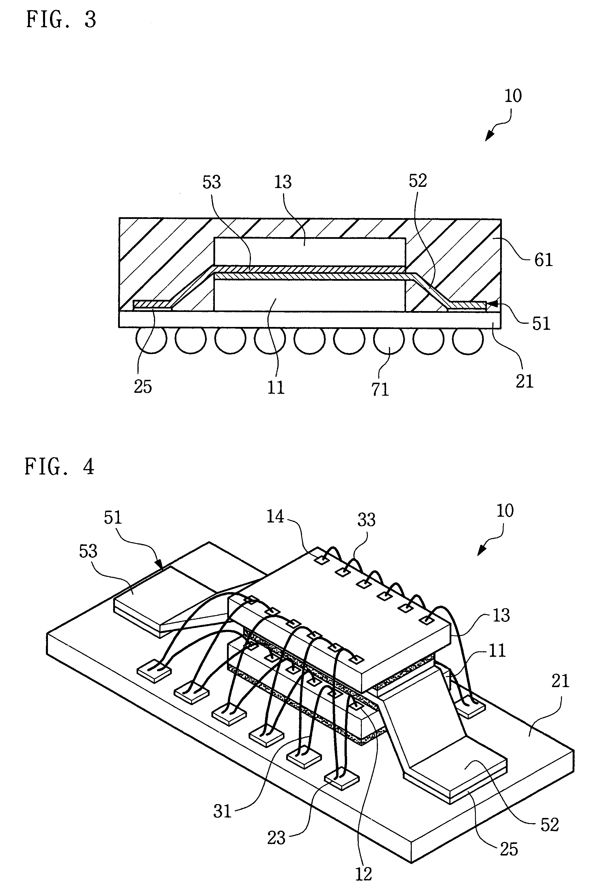
[0014] An exemplary embodiment of the present invention is directed to a semiconductor chip package which may prevent heat being trapped between semiconductor chips to improve thermal performance.
[0015] An exemplary embodiment of the present invention is directed to a semiconductor chip package which may enhance thermal performance corresponding to increased operating speed and high integration.
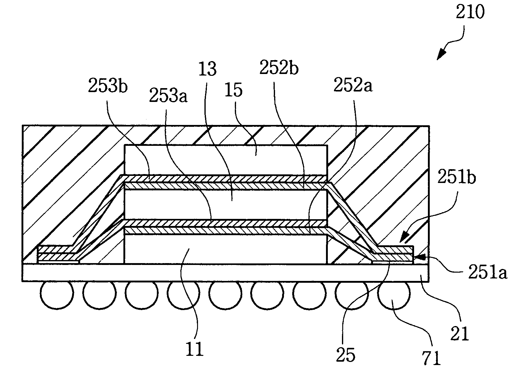
[0028] A semiconductor chip package with a thermoelectric cooler in accordance with still another exemplary embodiment of the present invention may include a module-type package having a plurality of semiconductor chip packages mounted on a substrate. Each semiconductor chip package may comprise a semiconductor chip, a substrate and an encapsulant. The semiconductor chip may be mounted on the substrate. The substrate may have circuit patterns. The encapsulant may protect the semiconductor chip. At least one semiconductor chip package may have a P-type material plate and an N-type material plate thereon. A portion of one of the P-type and N-type material plates may be attached to the encapsulant. The P-type and N-type material plates may be electrically connected with circuit patterns of the substrate to be provided with DC power.

Problems solved by technology

The conventional semiconductor chip package may have several disadvantages caused by thermal stresses.
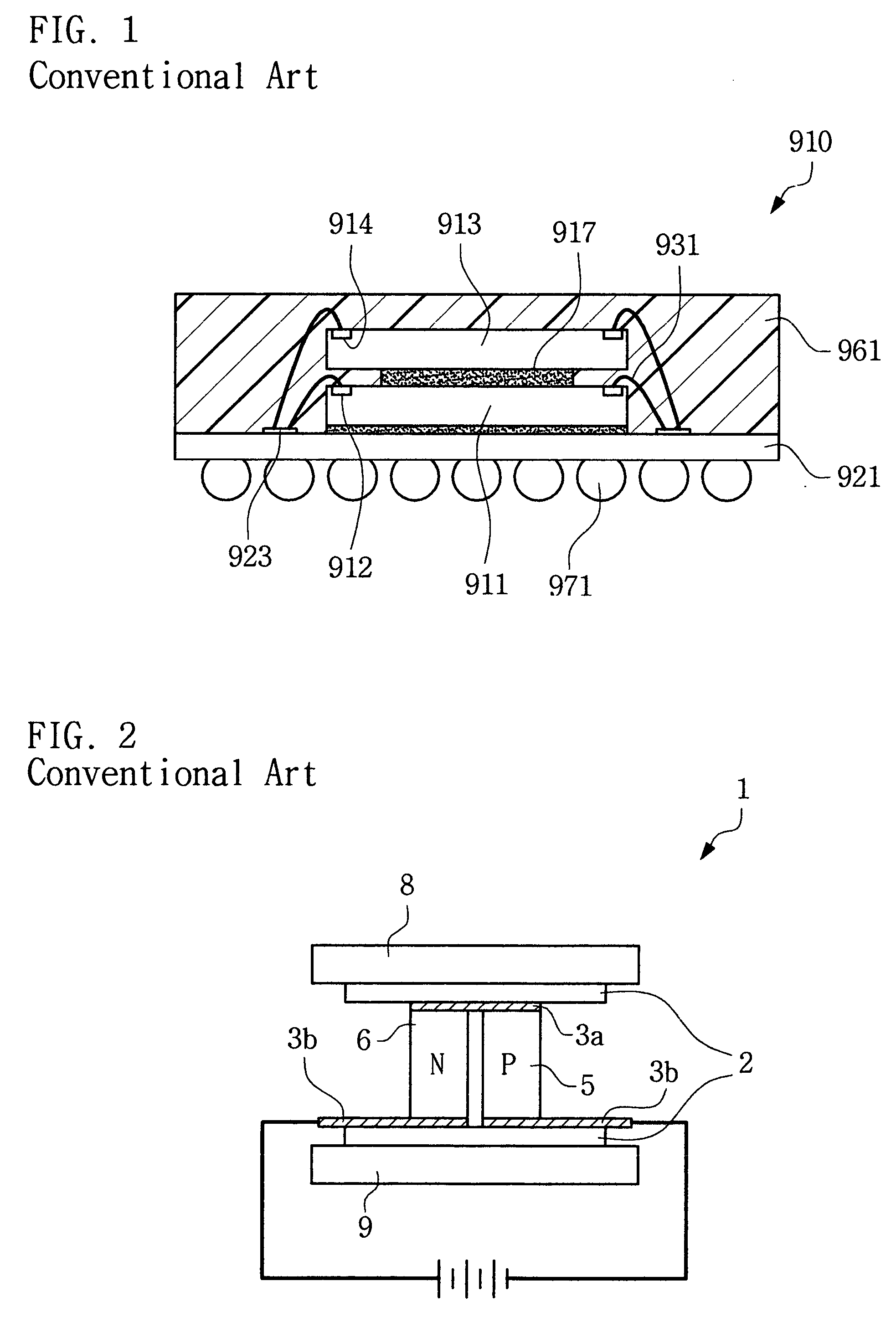
For example, in case of a multi-chip package having a spacer between semiconductor chips, release of heat between the chips may be difficult to realize.
With high-speed operation and high integration, the junction temperature of internal circuits of a semiconductor chip may increase, which may lead to an increased amount of heat generation.
If the increased amount of generated heat is released poorly, in the case of electronic equipment using a semiconductor chip package such as a mobile product, characteristics of the semiconductor chip package such as refresh characteristics, operating speed and cycle life may decrease.

Method used


Image

  • Semiconductor chip package with thermoelectric cooler
  • Semiconductor chip package with thermoelectric cooler
  • Semiconductor chip package with thermoelectric cooler

Examples


Embodiment Construction

[0044] The present invention will now be described more fully hereinafter with reference to the accompanying drawings, in which exemplary embodiments of the invention are illustrated. This invention may, however, be embodied in many different forms and should not be construed as limited to the particular embodiments set forth herein. Rather, these embodiments are provided so that this disclosure will be thorough and complete, and will fully convey the scope of the invention to those skilled in the art.

[0045] In the description, well-known structures and processes have not been described or illustrated in detail to avoid obscuring the present invention. It will be appreciated that for simplicity and clarity of illustration, some elements illustrated in the figures have not necessarily been drawn to scale. For example, the dimensions of some of the elements have been exaggerated or reduced relative to other elements for clarity.

[0046]FIG. 2 is a schematic view of a typical thermoele...


PUM


Abstract

The semiconductor chip package may include a substrate having circuit patterns and substrate pads connected with the circuit patterns. At least one semiconductor chip is mounted on the substrate, and a thermoelectric cooler having a P-type material plate and an N-type material plate is mounted on the semiconductor chip. Portions of the P-type and N-type material plates may be attached on the semiconductor chip. The P-type and N-type material plates may be electrically connected to the circuit patterns of the substrate to be provided with DC power.

Description

CROSS REFERENCE TO RELATED APPLICATIONS [0001] This U.S. non-provisional application claims priority under 35 U.S.C. §119 of Korean Patent Application No. 2004-51207, filed on Jul. 1, 2004, the entire contents of which are incorporated herein by reference. BACKGROUND OF THE INVENTION [0002] 1. Field of the Invention [0003] The present invention relates to a semiconductor device and, more particularly, to a semiconductor device having a thermoelectric cooler (TEC). [0004] 2. Description of the Related Art [0005] With the development of semiconductor technology, and the pressing demand of users, recent trends in the electronics industry are towards minimization, light-weight construction and multi-function. To meet these demands, multi-chip packaging techniques have been introduced. Multi-chip packages (MCPs) include a plurality of semiconductor chips in a single package. MCPs manufactured by such techniques are advantageous in size, weight and mounting area over those including a plu...

Claims


Application Information

Patent Timeline
Patent Type & Authority Applications(United States)
IPC IPC(8): H01L23/02
CPCH01L23/38H01L2924/19107H01L2224/16H01L2224/32145H01L2224/32225H01L2224/48091H01L2224/48227H01L2224/49112H01L2224/73253H01L2224/73265H01L2225/06589H01L2924/15311H01L25/0657H01L2224/16225H01L24/49H01L24/48H01L2924/00014H01L2924/00H01L24/40H01L2224/05553H01L2224/05554H01L2224/49113H01L2924/10161H01L2224/37599H01L2224/8385H01L2224/8485H01L24/41H01L24/37H01L2924/181H01L24/84H01L2224/45099H01L2224/45015H01L2924/207H01L2224/37099H01L2924/00012H01L2224/73221H01L23/34H01L23/48
Inventor LEE, HAE-HYUNGPARK, SANG-WOOKBAEK, JOONG-HYUNLEE, DONG-HOLEE, JIN-YANG
Owner SAMSUNG ELECTRONICS CO LTD
Learn More