Semiconductor chip package and method for making the same

a technology of semiconductor and chip, applied in the direction of semiconductor/solid-state device details, electrical apparatus, semiconductor devices, etc., can solve the problem that the active surface 104/b> of the microelectronic chip generally does not provide enough surface for all external contacts, and achieves the effect of reducing the cost of wafers, saving labor hours, and increasing throughpu

Active Publication Date: 2006-05-09
ADVANCED SEMICON ENG INC
View PDF7 Cites 71 Cited by
  • Summary
  • Abstract
  • Description
  • Claims
  • Application Information

AI Technical Summary

Benefits of technology

[0010]The semiconductor chip packages disclosed in the present invention are characterized in that the external contacts may be positioned over the active area and the dummy area thereby the semiconductor chip package may be designed to have a “fan-out” or “fan-in” layout to provide enough surface for the external contacts. Furthermore, since the dummy area is a portion of the chip and is formed from semiconductor material with good heat dissipation capability, the dummy area may function as a heat sink to help heat dissipation of the chip thereby enhancing the thermal performance of the semiconductor chip package. According to the aforementioned advantages, the semiconductor chip package of the present invention provides a larger distributing surface for the external contacts and has a better thermal performance, and, therefore, is a suitable design for high packaging density (high pin count) semiconductor chip packages.
[0016]The semiconductor chip package manufacturing methods disclosed in the present invention are accomplished by directly forming a substrate structure for making external electrical connection on the surface of a semiconductor wafer via build-up or lamination process whereby a plurality of semiconductor chip packages are manufactured at one time thereby saving save labor hours and increasing throughput. As the cost of wafer is decreased and the size of wafer is increased, the methods of the present invention are suitable in packaging a semiconductor chip having the aforementioned active area and dummy area into a semiconductor chip package having a “fan-out” or “fan-in” layout by electrically connecting the bonding pads disposed on the active area to the external contacts positioned over the active area and the dummy area.

Problems solved by technology

However, in such kind of chip scale package, the surface area provided by the active surface 104 of the microelectronic chip generally does not provide enough surface for all of the external contacts needed to contact the external component.

Method used


Image

  • Semiconductor chip package and method for making the same
  • Semiconductor chip package and method for making the same
  • Semiconductor chip package and method for making the same

Examples


Embodiment Construction

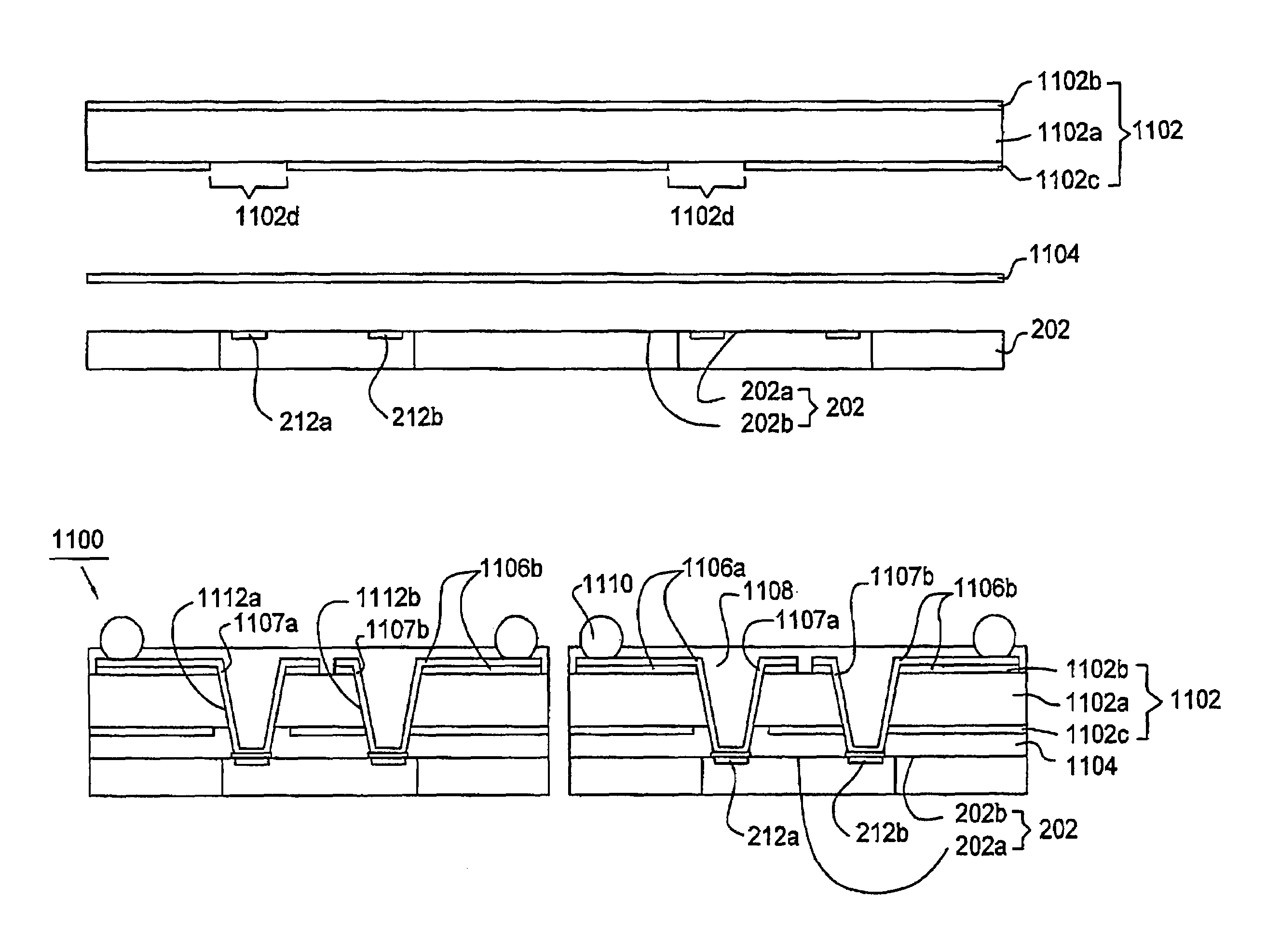
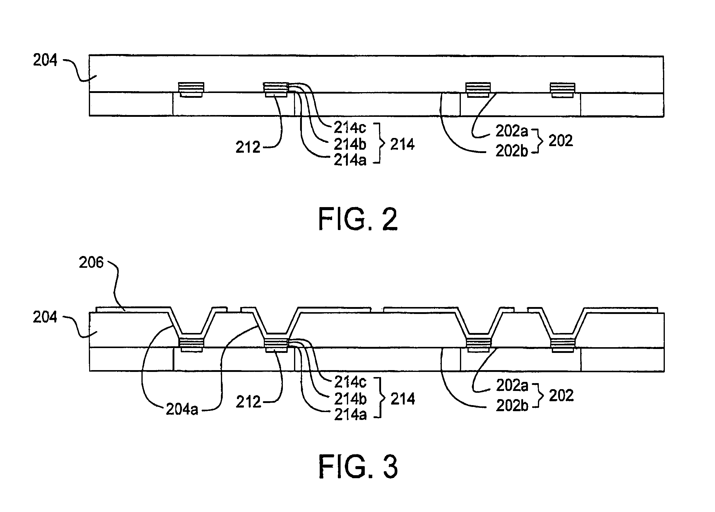
[0022]FIG. 5 shows semiconductor chip packages 200 according to one embodiment of the present invention. The semiconductor chip package 200 mainly comprises a semiconductor chip 202, a dielectric layer 204 disposed on the semiconductor chip 202, a plurality of conductive traces 206 electrically connected to the semiconductor chip 202, a dielectric layer 208 disposed on the conductive traces 206 and the dielectric layer 204 and a plurality of external contacts 210 formed on the conductive traces 206 exposed from the dielectric layer 208.

[0023]The semiconductor chip 202 has a surface including an active area 202a, a dummy area 202b surrounding the active area 202a. The upper surface of the semiconductor chip 202 is provided with a plurality of bonding pads 212, e.g., aluminum pads or copper pads, disposed on the active area 202a of the semiconductor chip 202. The bonding pads 212 are electrically connected to the internal integrated circuit of the chip. The bonding pads 212 are electr...


PUM


Abstract

A semiconductor chip package mainly includes a semiconductor chip, a first dielectric layer disposed on the semiconductor chip, a plurality of conductive traces electrically connected to the semiconductor chip, a second dielectric layer disposed on the conductive traces and the first dielectric layer wherein a portion of the conductive traces are exposed from the second dielectric layer, and a plurality of contacts for external connection formed on the exposed portion of the conductive traces. The semiconductor chip has a surface including an active area, a dummy area surrounding the active area, and a plurality of bonding pads disposed on the active area. The bonding pads are electrically connected to the contacts by the conductive traces. The present invention further provides methods for manufacturing the semiconductor chip package.

Description

[0001]This application claims the priority benefit of Taiwan Patent Application Serial Number 092123767, filed Aug. 28, 2003, the full disclosure of which is incorporated herein by reference.BACKGROUND OF THE INVENTION[0002]1. Field of the Invention[0003]This invention relates to a semiconductor chip package.[0004]2. Description of the Related Art[0005]Higher performance, lower cost, increased miniaturization of integrated circuit components, and greater packaging density of integrated circuits are ongoing goals of the computer industry. As these goals are achieved, microelectronic chips become smaller. Of course, the goal of greater packaging density requires that the entire microelectronic chip package be equal to or only slightly larger (about 10% to 30%) than the size of the microelectronic chip itself. Such microelectronic chip package is called a “chip scale package (CSP)”.[0006]As shown in FIG. 1, a conventional chip scale package comprises a microelectronic chip 102 and a bu...

Claims


Application Information

Patent Timeline
Patent Type & Authority Patents(United States)
IPC IPC(8): H01L21/44H01L21/4763H01L23/538
CPCH01L23/5389H01L24/97H01L24/19H01L2924/01087H01L2224/04105H01L2224/20H01L2224/97H01L2924/01013H01L2924/01029H01L2924/01078H01L2924/14H01L2924/15311H01L2924/18162H01L2924/01033H01L2924/01023H01L2924/01005H01L2224/82H01L2924/12042H01L2224/12105H01L2224/023H01L2924/00H01L2924/0001
Inventor CHAO, SHIN HUAFANG, JEN KUANGTONG, HO MING
Owner ADVANCED SEMICON ENG INC
Why Eureka
Try Eureka