Plasma display panel

a technology of display panel and plasma, which is applied in the manufacture of electrode systems, electric discharge tubes/lamps, gas discharge sealing, etc., can solve the problems of deteriorating the quality of display operation, low noise level at audible frequency, and abnormal noise, so as to prevent the generation of noise due to malcontact

Inactive Publication Date: 2006-01-05
FUJITSU HITACHI PLASMA DISPLAY LTD
View PDF3 Cites 15 Cited by
  • Summary
  • Abstract
  • Description
  • Claims
  • Application Information

AI Technical Summary

Benefits of technology

[0012] According to the present invention, a sealing material containing non-porous bead spacers is used for sealing the front substrate and the rear substrate that are opposed to each other defining a discharge gas space. A “non-porous bead” in the present invention means a bead having a small value of specific surface area such that the viscosity of the sealing paste to be the sealing material is not altered substantially when the beads are added into the sealing material.
[0013] According to the present invention, the thickness of the plasma display panel can be made uniform along the entire perimeter of the sealing portion between the front substrate and the rear substrate, so that an appropriate contact between the front substrate and the rear substrate can be obtained along the entire perimeter inside the sealing portion. Thus, generation of a noise due to the malcontact can be prevented.

Problems solved by technology

The malcontact between the front substrate and the rear substrate inside the sealing portion may cause an abnormal noise during a display operation.
When a high frequency drive voltage is applied for a display, periodical electrostatic attraction may vibrate the glass substrates locally, so that a low level of noise at an audible frequency is generated.
This noise may deteriorate quality of display operation.
If a quantity of the spacers is insufficient, the spacers may be broken by an excessive pressure per spacer.
However, a classification work for obtaining glass beads of a sharp distribution of granularity causes increase of cost of the glass beads.
It is difficult to remove smaller particles compared with removal of larger particles than a desired size.

Method used


Image

  • Plasma display panel
  • Plasma display panel
  • Plasma display panel

Examples


Embodiment Construction

[0024] Hereinafter, the present invention will be explained more in detail with reference to embodiments and drawings.

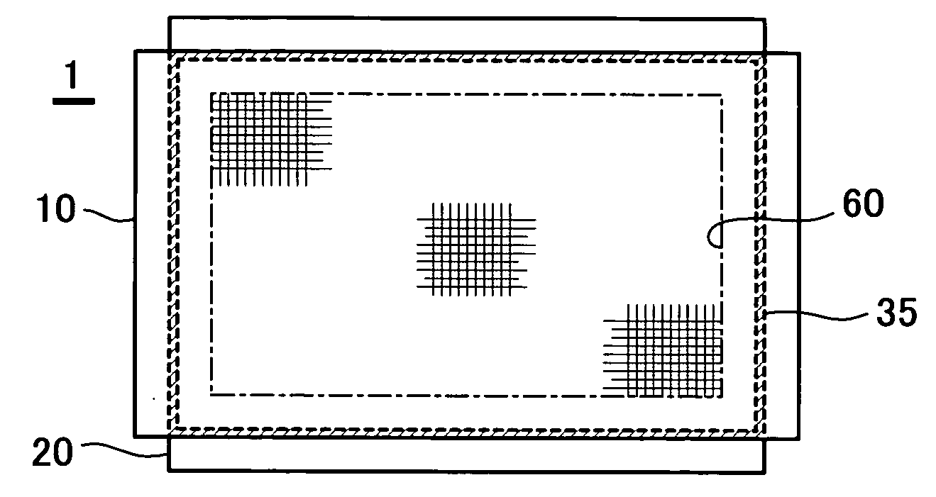
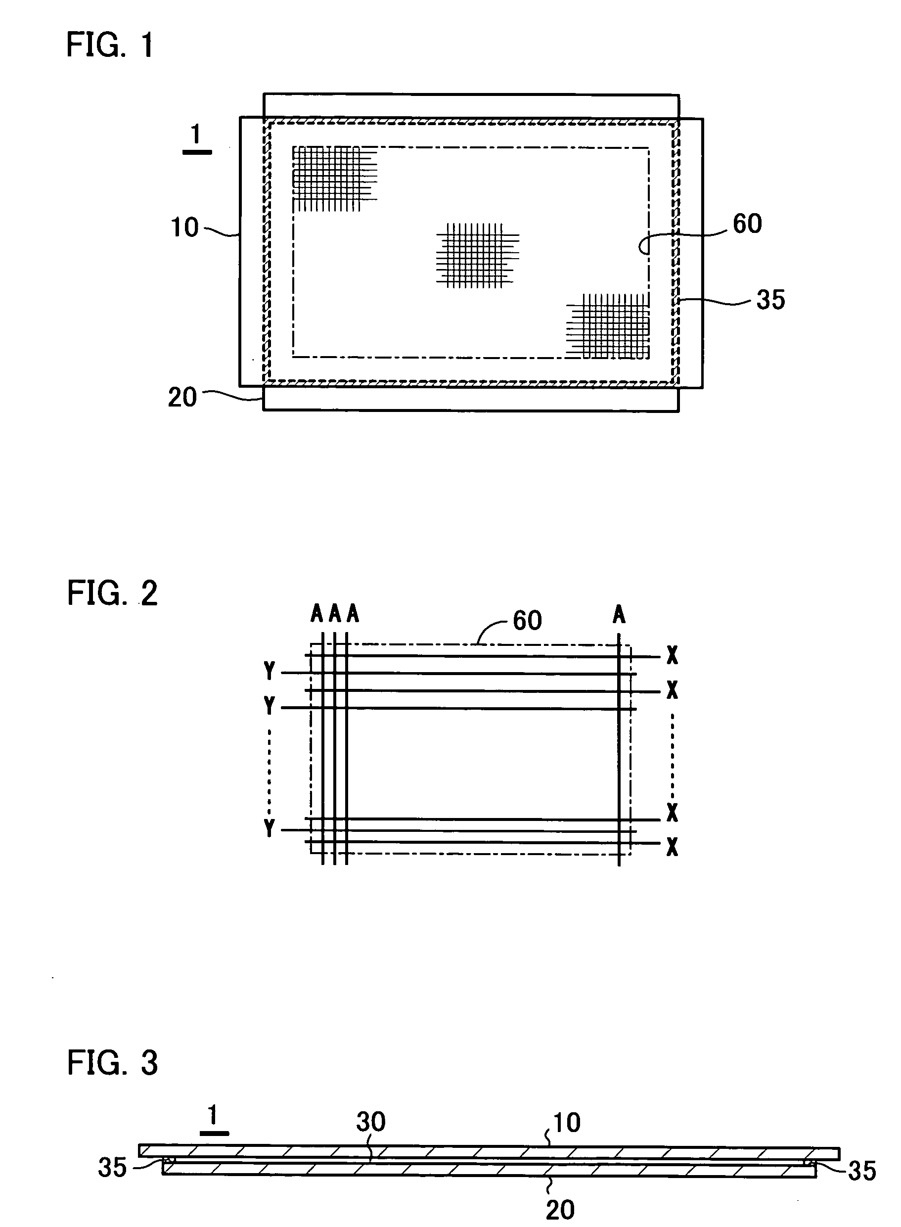
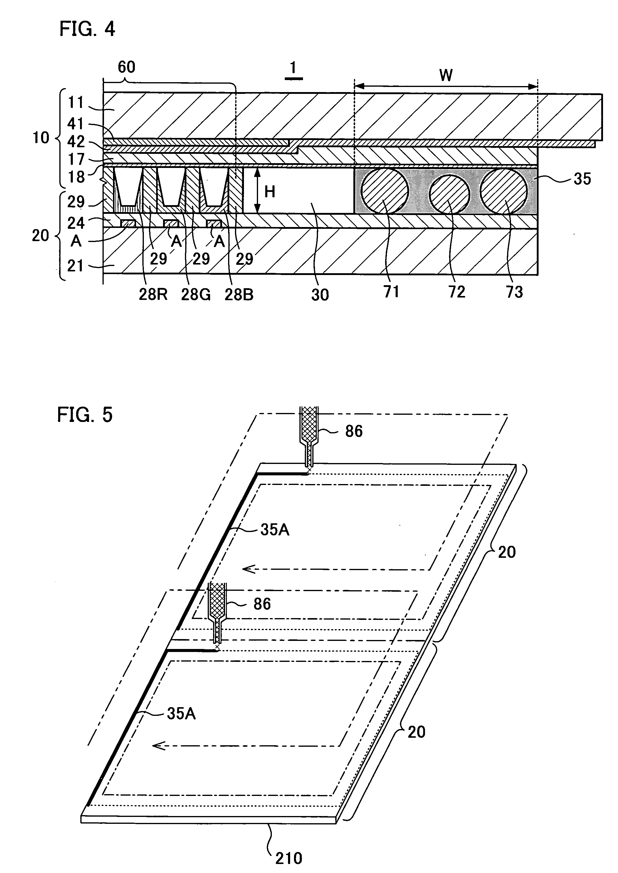
[0025]FIG. 1 shows a general structure of a plasma display panel. The plasma display panel 1 includes a front substrate 10 and a rear substrate 20, which constitutes a screen 60 made of plural discharge cells arranged in a matrix. Each of the front substrate 10 and the rear substrate 20 has a structural body including a glass substrate that is larger than the screen 60 and has a thickness of approximately 3 millimeters, on which electrodes and other elements are arranged. The front substrate 10 and the rear substrate 20 are overlapped so as to be opposed to each other and are sealed at their peripheral portions surrounding their overlapped portions by using a sealing material 35 that has a frame-like shape in a plan view. As shown in FIG. 1, the front substrate 10 extends from right and left sides of the rear substrate 20 by approximately 5 millimeters, while the re...


PUM


Abstract

A plasma display panel includes a front substrate and a rear substrate that are opposed to each other with a discharge gas space between them, and a sealing material for sealing the front substrate and the rear substrate at their peripheral portions. The sealing material contains an appropriate quantity of spacers so that a thickness of the plasma display panel is uniform along the entire perimeter of the sealing portion between the front substrate and the rear substrate. The sealing material contains non-porous beads as the spacers, preferably at a ratio within the range of 0.05-2.0 wt %.

Description

BACKGROUND OF THE INVENTION [0001] 1. Field of the Invention [0002] The present invention relates to a plasma display panel (PDP), which is characterized in a structure of a sealing material that is used for sealing a front substrate and a rear substrate. [0003] 2. Description of the Prior Art A plasma display panel includes a front substrate and a rear substrate, which are both larger than a screen. The front substrate and the rear substrate are opposed to each other and sealed with a sealing material that is arranged at the outer portion of the screen and has a frame-like shape so that a closed discharge gas space is defined by them. The front substrate and the rear substrate are glass substrates, while the sealing material is a burned material of low melting point glass. [0004] Among plasma display panels having such a structure, a surface discharge type plasma display panel for use as a color display includes partitions that prevent discharge interference between neighboring cel...

Claims


Application Information

Patent Timeline
Patent Type & Authority Applications(United States)
IPC IPC(8): H01J17/49H01J9/26H01J11/24H01J11/46H01J11/48
CPCH01J9/261H01J11/48H01J11/12
Inventor NONOMURA, MINAHIROYANAGIHARA, NAOTOSETO, MASAYUKIUKAI, YOSHITAKAMURA, RYOUICHI
Owner FUJITSU HITACHI PLASMA DISPLAY LTD
Why Eureka
Try Eureka