Wafer dividing method

a technology of dividing method and wafer, which is applied in the direction of basic electric elements, electrical apparatus, semiconductor devices, etc., can solve problems such as chipping, and achieve the effect of improving the dividing method and avoiding the chipping of semiconductor devices

Active Publication Date: 2006-01-05
DISCO CORP
View PDF3 Cites 36 Cited by
  • Summary
  • Abstract
  • Description
  • Claims
  • Application Information

AI Technical Summary

Benefits of technology

[0005] It is an object of the present invention, therefore, to improve the wafer dividing method in the mode called dicing-before-grinding so that chipping of the semiconductor device can be avoided.

Problems solved by technology

Owing to such vibrations, chipping takes place particularly at the corner of the semiconductor device.

Method used


Image

  • Wafer dividing method
  • Wafer dividing method
  • Wafer dividing method

Examples


Embodiment Construction

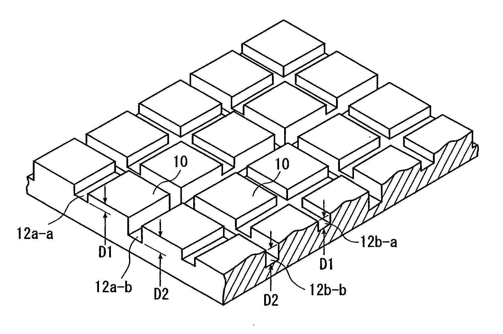
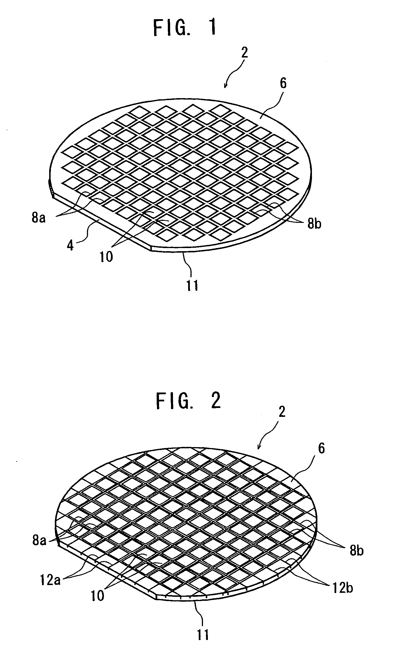
[0018]FIG. 1 shows an example of a wafer to which the wafer dividing method of the present invention is applied. The illustrated wafer entirely indicated at the numeral 2, which may be a silicon wafer, is of a thin disk shape as a whole, and has an arcuate edge, except a straight edge 4 called an orientation flat. On the face 6 of the wafer 2, a plurality of rectangular regions 10 are defined by a first set of plural streets 8a and a second set of plural streets 8b. The first set of the streets 8a extend parallel to each other, and the second set of the streets 8b also extend parallel to each other. The second set of the streets 8b extend perpendicularly to the first set of the streets 8a. A suitable circuit element is disposed in each of the rectangular regions 10.

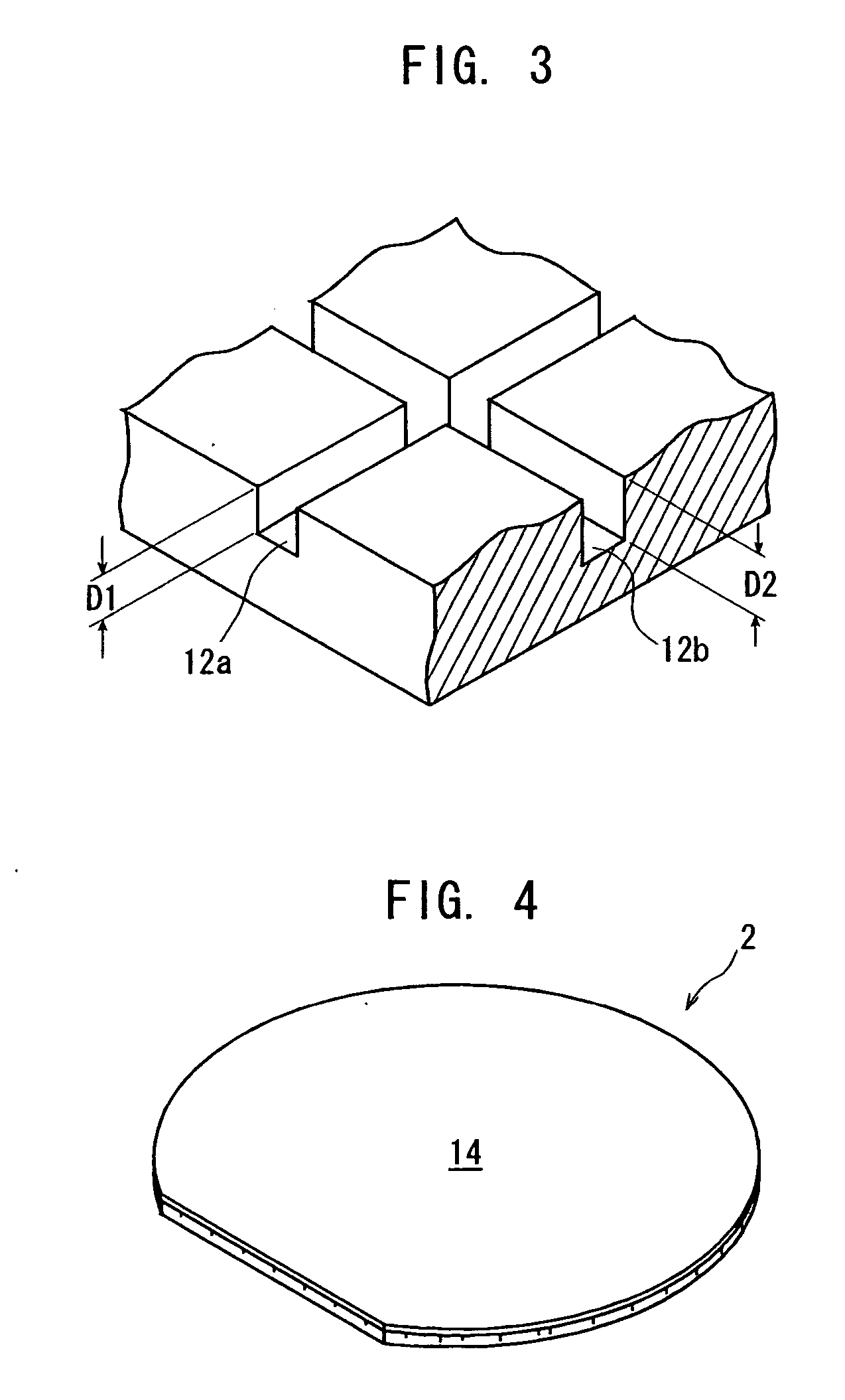
[0019] In the wafer dividing method of the present invention, as shown in FIG. 2, a groove forming step of forming grooves 12a and 12b along the streets 8a and 8b on the face 6 of the wafer 2 is performed before the back...


PUM


Abstract

A wafer dividing method for dividing a wafer along a first set of plural streets extending parallel to each other, and a second set of plural streets extending parallel to each other and extending perpendicularly to the first set of the streets, the wafer having a plurality of rectangular regions defined on the face thereof by these streets. The wafer dividing method includes a groove forming step of forming grooves along the streets on the face of the wafer, and a grinding step of grinding the back of the wafer after the groove forming step. The grooves formed by the groove forming step include grooves having a first depth D1, and grooves having a second depth D2 which is greater than the first depth D1 (D2>D1).

Description

FIELD OF THE INVENTION [0001] This invention relates to a wafer dividing method for dividing a wafer along a first set of plural streets extending parallel to each other, and a second set of plural streets extending parallel to each other and extending perpendicularly to the first set of the streets, the wafer having a plurality of rectangular regions defined on the face thereof by the first set of the streets and the second set of the streets. More particularly, the present invention relates to a wafer dividing method arranged to divide the wafer in a mode called dicing-before-grinding, namely, a mode including a groove forming step of forming grooves along the streets on the face of the wafer, and a grinding step of grinding the back of the wafer after the groove forming step. DESCRIPTION OF THE PRIOR ART [0002] In the production of a semiconductor device, a plurality of rectangular regions are defined on the face of a wafer by streets arranged in a lattice pattern, namely, a firs...

Claims


Application Information

Patent Timeline
Patent Type & Authority Applications(United States)
IPC IPC(8): H01L21/301H01L21/302
CPCH01L21/6836H01L2221/68327H01L21/78
Inventor OKADA, JUN
Owner DISCO CORP
Why Eureka
Try Eureka