Data processing method, semiconductor device for detecting physical quantity distribution, and electronic apparatus

a semiconductor device and data processing technology, applied in the field of data processing method, semiconductor device for detecting physical quantity distribution, electronic apparatus, can solve the problem that the video signals that should be output from the solid state imaging device cannot be obtained together with the computed signals

Inactive Publication Date: 2006-01-19
SONY CORP
View PDF3 Cites 88 Cited by
  • Summary
  • Abstract
  • Description
  • Claims
  • Application Information

AI Technical Summary

Benefits of technology

[0028] In view of the above-described circumstances, it is an object of the present invention to provide a simpler mechanism that allows computed data to be output, together with video signals, as multi-level digital data.

Problems solved by technology

In the known mechanisms for performing the above-described processing, only the computed signals are output from the solid state imaging device, and thus, video signals that should be output from the solid state imaging device cannot be obtained together with the computed signals.

Method used


Image

  • Data processing method, semiconductor device for detecting physical quantity distribution, and electronic apparatus
  • Data processing method, semiconductor device for detecting physical quantity distribution, and electronic apparatus
  • Data processing method, semiconductor device for detecting physical quantity distribution, and electronic apparatus

Examples


first embodiment

Spatial Addition Processing Operation

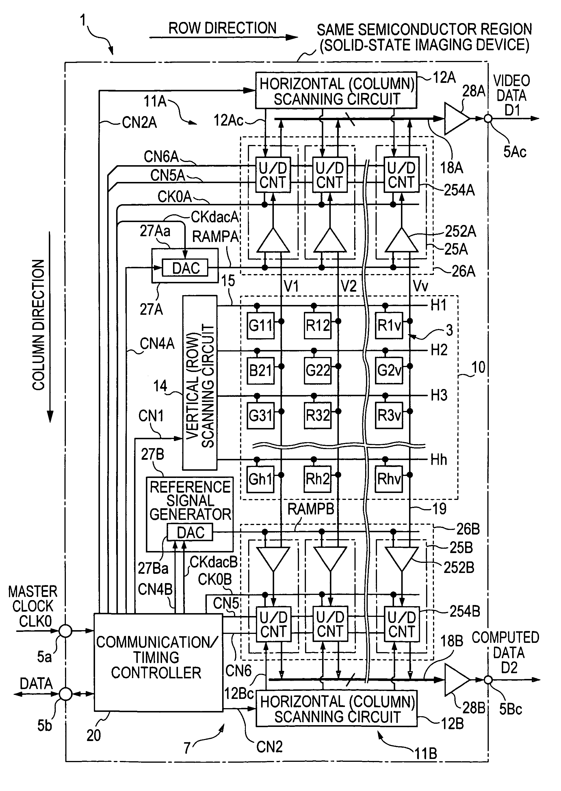
[0193]FIG. 5 is a timing chart illustrating the spatial addition processing operation performed by the column AD circuit 25B in the computed data processor 11B of the solid state imaging device 1 of the first embodiment shown in FIG. 1. It should be assumed that a color separation filter is not disposed in the pixel portion 10 and monochromatic imaging is performed.

[0194] The spatial addition processing is addition processing between a plurality of pixel signals located at different pixel positions in one field of an image which is captured substantially at the same time. Typical examples of the spatial addition processing include vertical-column addition processing performed on pixel signals of a plurality of (may be 3 or more) adjacent rows and horizontal-row addition processing performed on pixel signals at a plurality of (may be three or more) adjacent pixel positions in the same row. The spatial addition processing of the first embodiment ...

second embodiment

Spatial Difference Processing Operation by Solid State Imaging Device

[0220]FIG. 8 is a timing chart illustrating the operation of the spatial difference processing operation in the column AD circuit 25 of the solid state imaging device 1 of the second embodiment shown in FIG. 6. In this case, a color separation filter is not disposed in the pixel portion 10, and monochromatic imaging is performed.

[0221] In the second embodiment, as shown in FIG. 7, since the count value indicating the previous subtraction processing result is transferred to the data storage unit 256 before the first readout operation (AD conversion) for the pixel signal to be processed, the readout operation is not restricted.

[0222] The timing chart illustrating the spatial addition processing in the solid state imaging device 1 of the second embodiment is not shown. However, as described with reference to FIG. 5, the combination of the count modes for the reset components ΔV and the signal components Vsig during...

third embodiment

Temporal Difference Processing Operation

[0302]FIG. 14 is a timing chart illustrating the temporal difference processing operation performed by the column AD circuit 25 of the solid state imaging device 1 of the third embodiment shown in FIG. 11. FIG. 15 is a timing chart illustrating the temporal difference processing operation in relation to the frame rate. A description is given below by separating the temporal difference operation into the temporal difference output operation by the computed data processor 11B and the normal video output operation by the normal data processor 11A.

[0303] Temporal Difference Output Operation

[0304] It can be considered that the operation timing in the temporal difference processing shown in FIG. 14 is performed by substituting the n−1 row (previous row) and the n row (current row) in the spatial difference processing of the second embodiment shown in FIG. 8 by the n−1 frame (previous frame) and the n frame (current frame), respectively.

[0305] Th...


PUM


Abstract

A data processing apparatus and method is disclosed for obtaining digital data for a plurality of signals to be processed, comprising. The disclosed process includes comparing, by using digital data for a first signal of the plurality of signals, an electric signal corresponding to a second signal of the plurality of signals with a reference signal; obtaining digital data for the second signal based on the comparing step; performing a counting operation in one of a down-counting mode and an up-counting mode while the comparing step is being performed; storing a first count value; outputting the first count value as computed data at a predetermined time; generating normal data based on one of the plurality of signals to be processed; and outputting the normal data.

Description

CROSS PREFERENCE TO RELATED APPLICATIONS [0001] The present invention claims the benefit of Japanese Patent Application JP 2004-209887 filed in the Japanese Patent Office on Jul. 16, 2004, the entire contents of which are incorporated herein by reference. FIELD OF THE INVENTION [0002] The present invention relates to a data processing method, a data processing apparatus, a semiconductor device for detecting the physical quantity distribution in which a plurality of unit elements are disposed, and an electronic apparatus. More particularly, the invention relates to a digital signal processing technology suitably used for semiconductor devices for detecting the physical quantity distribution, for example, solid state imaging devices, and other electronic apparatuses, in which a plurality of unit elements responsive to electromagnetic waves, such as light or radiation, input from an external source, are disposed, and the physical quantity distribution obtained by converting electromagn...

Claims


Application Information

Patent Timeline
Patent Type & Authority Applications(United States)
IPC IPC(8): H04N3/14H04N5/335H04N5/355H04N5/357H04N5/374H04N5/378
CPCH04N5/335H04N3/155H04N25/46H04N25/616H04N25/75H04N25/78
Inventor NITTA, YOSHIKAZUFUKUSHIMA, NORIYUKIMURAMATSU, YOSHINORIYASUI, YUKIHIRO
Owner SONY CORP
Why Eureka
Try Eureka