Wideband antenna and communication apparatus having the antenna

a communication apparatus and antenna technology, applied in the structure of resonant antennas, antennas with plural divergent straight elements, radiating elements, etc., can solve the problem of insufficient extension of the transmitting and receiving band in the required frequency band

Active Publication Date: 2006-01-26
TOSHIBA CLIENT SOLUTIONS CO LTD
View PDF10 Cites 22 Cited by
  • Summary
  • Abstract
  • Description
  • Claims
  • Application Information

AI Technical Summary

Problems solved by technology

However, the transmitting and receiving band in a required frequency band may not be sufficiently extended merely by unconditionally forming the structure disclosed by U.S. Pat. No. 4,843,403.

Method used


Image

  • Wideband antenna and communication apparatus having the antenna
  • Wideband antenna and communication apparatus having the antenna
  • Wideband antenna and communication apparatus having the antenna

Examples


first embodiment

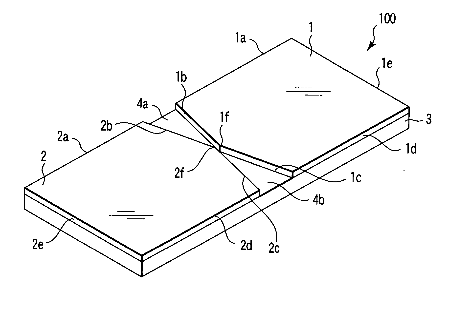
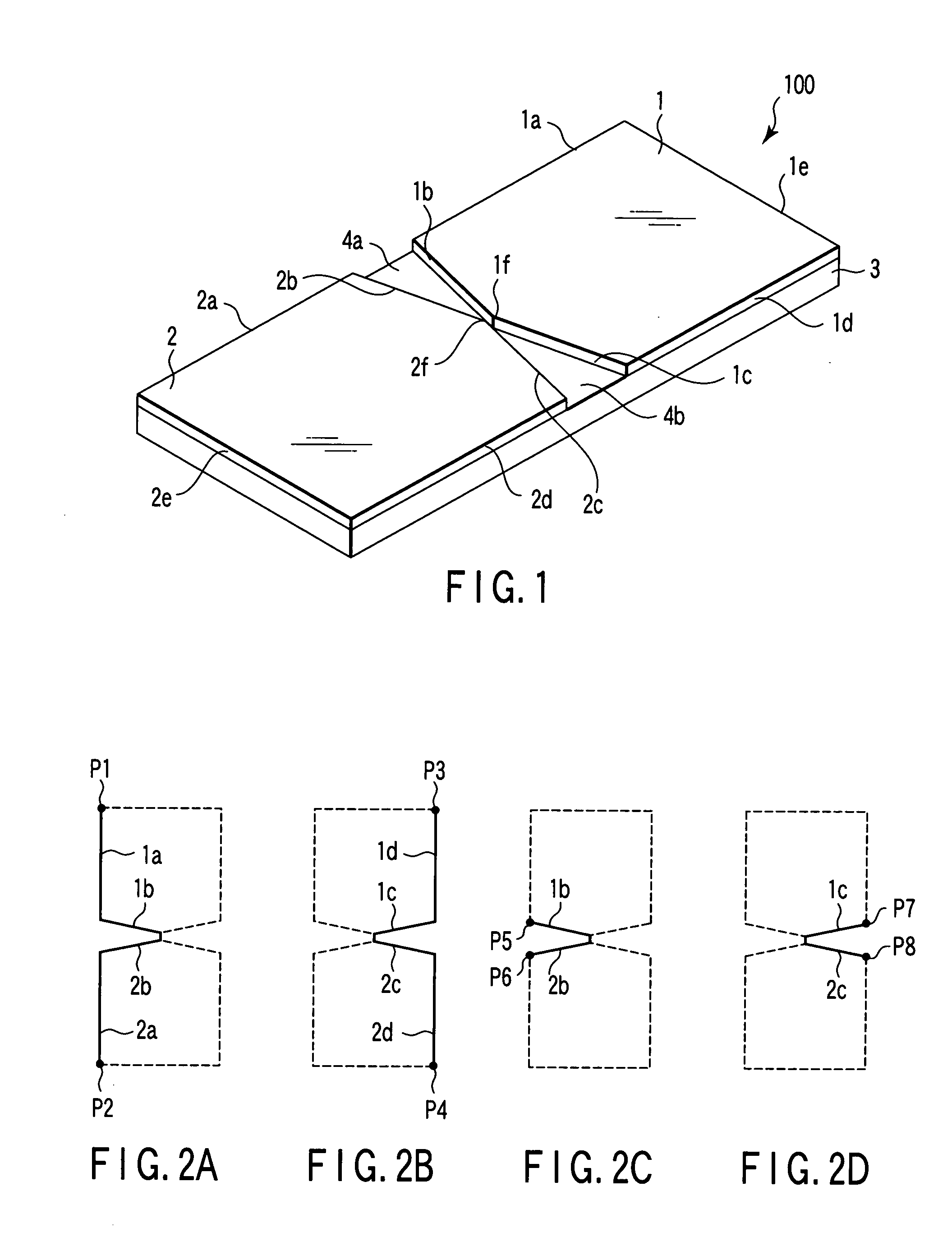
[0081]FIG. 1 is the perspective view showing the structure of the wideband antenna 100 regarding the first embodiment of the invention.

[0082] As shown in FIG. 1, the antenna 100 comprises the conductive elements 1, 2 and a dielectric substrate 3.

[0083] The elements 1, 2 are thin plates made of conductive material. The elements 1, 2 respectively have a pentagonal shape formed so that one side of a rectangular thin plate is linearly notched with the same angle from its center to both sides. The shapes of the elements 1, 2 are approximately congruent with each other.

[0084] Five sides of the element 1 are referred to as sides 1a, 1b, 1c, 1d and 1e as shown FIG. 1. The sides 1b, 1c are inclined sides provided with a shape so as to notch as mentioned above and contact each other. A top 1f is formed at a part at which the sides 1b, 1c contact with each other. The side 1a contacts the side 1b. The side 1d contacts the side 1c. The side 1e contacts the sides 1a, 1d, respectively.

[0085] F...

second embodiment

[0105]FIG. 9 is the illustration showing the structure of the wideband antenna 200 regarding the second embodiment of the invention. In FIG. 9, the same parts as those of FIG. 1 designated by the same reference numerals and detailed explanation thereof will be omitted.

[0106] As shown in FIG. 9, the antenna 200 comprises conductive elements 7 and 8. These elements 7, 8 are mounted on a dielectric substrate, but the substrate is not shown.

[0107] The elements 7, 8 are thin plates made of conductive material. The elements 7, 8 respectively have a pentagonal shape formed so that a first side of a rectangular thin plate is linearly notched with the same angle from its center to both sides and so that a second side facing the first side is linearly notched from one end of the second side. The shapes of the elements 7, 8 are approximately congruent with each other.

[0108] Five sides of the element 7 are referred to as sides 7a, 7b, 7c, 7d and 7e as shown in FIG. 9. Five sides of the eleme...

third embodiment

[0114]FIG. 13 is an illustration showing the structure of the wideband antenna 300 regarding the third embodiment of the invention. In FIG. 13 the same parts as that of FIG. 1 designated by the same reference numerals and detailed explanation thereof will be omitted.

[0115] As shown in FIG. 13, the antenna 300 comprises the elements 2 and an element 9. These elements 2, 9 are mounted on a dielectric substrate, but the substrate is not shown in FIG. 13. That is, the antenna 300 is equipped with the element 9 instead of the element 1 of the antenna 100.

[0116] The element 9 is a thin plate made of conductive material. The element 9 has a shape in which a part of the element 1 is notched in rectangle from the side of the side 1e of the element 1 and a notch 9a is provided. The element 9 is arranged opposite to the element 2 in the same positional relationship.

[0117] The element 9 has the sides 1a, 1b, 1c, 1d and the top 1f of the element 1 as they are. These sides are in the same posi...


PUM


Abstract

A wideband antenna in which a first and second conductive element are arranged so that a notch is formed between the first and second conductive element, wherein the first and second conductive element have shapes satisfying two conditions (i) a sum of the lengths of sides facing the notch and a first side terminating at one edge of a wider opening of the notch, these sides pertaining to the first conductive element, and the lengths of sides facing the notch and a second side terminating at one edge of the wider opening, these sides pertaining to the second conductive element, is approximately half of a first wavelength, and (ii) a sum of the lengths of sides pertaining to the first conductive element and facing the notch, and the lengths of sides pertaining to the second conductive element and facing the notch is approximately half of a second wavelength.

Description

CROSS-REFERENCE TO RELATED APPLICATIONS [0001] This application is based upon and claims the benefit of priority from prior Japanese Patent Applications No. 2004-205042, filed Jul. 12, 2004; No. 2005-004196, filed Jan. 11, 2005; and No. 2005-045783, filed Feb. 22, 2005, the entire contents of all of which are incorporated herein by reference. BACKGROUND OF THE INVENTION [0002] 1. Field of the Invention [0003] The present invention relates to a wideband antenna for transmitting and receiving radio waves and a communication apparatus having the antenna. [0004] 2. Description of the Related Art [0005] An antenna having a structure in which two metal elements are disposed opposite to each other so that a gap is interposed between them is disclosed. (Refer to U.S. Pat. No. 4,843,403) [0006] However, the transmitting and receiving band in a required frequency band may not be sufficiently extended merely by unconditionally forming the structure disclosed by U.S. Pat. No. 4,843,403. BRIEF S...

Claims


Application Information

Patent Timeline
Patent Type & Authority Applications(United States)
IPC IPC(8): H01Q9/28H01Q1/24H01Q1/36H01Q1/38H01Q5/00H01Q5/10H01Q5/364H01Q9/26H01Q9/44H01Q13/10
CPCH01Q1/38H01Q5/364H01Q9/285
Inventor SHIMASAKI, HIROSHIMIZOGUCHI, SATOSHITESHIMA, MASAO
Owner TOSHIBA CLIENT SOLUTIONS CO LTD
Why Eureka
Try Eureka