Wafer boat for reducing wafer warpage

a technology of warpage boat and wafer, which is applied in the field of furnaces, can solve the problems of warpage of wafer, large amount of process gas consumed by apcvd system, and often exhibit poor step coverage, so as to particle generation, prevent or substantially reduce the warpage of wafer during processing, and minimize the contact surface area

Inactive Publication Date: 2006-02-09
TAIWAN SEMICON MFG CO LTD
View PDF14 Cites 18 Cited by
  • Summary
  • Abstract
  • Description
  • Claims
  • Application Information

AI Technical Summary

Benefits of technology

[0016] In accordance with these and other objects and advantages, the present invention is generally directed to a wafer boat which is suitable for eliminating or at least reducing wafer warpage and particle generation during the furnace processing of wafers, for example. The wafer boat typically includes a base plate and multiple vertical support rods extending from the base plate. Multiple, vertically-spaced wafer support pins extend from each support rod, and wafer support pins on the respective support rods support a corresponding one of the wafers during processing. The upper surface of each wafer support pin is disposed at an acute angle with respect to the longitudinal axis of the support rod to minimize the contact surface area of each wafer support pin with the backside of the wafer, reducing the accumulation of particles between the wafer support pin and the wafer. Furthermore, the wafer support pins support each wafer at or near the center of gravity of the wafer, preventing or substantially reducing warpage of the wafer during processing.

Problems solved by technology

While APCVD systems have high equipment throughput, good uniformity and the capability to process large-diameter wafers, APCVD systems consume large quantities of process gas and often exhibit poor step coverage.
This tends to induce stress on the edge of the wafer 29, causing warpage of the wafer 29 and negatively impacting subsequent photolithography processes.
Another drawback associated with the conventional wafer boat 24 is that the total surface area of the pin contact points 31 on each wafer 29 is typically about 400 mm2.

Method used


Image

  • Wafer boat for reducing wafer warpage
  • Wafer boat for reducing wafer warpage
  • Wafer boat for reducing wafer warpage

Examples


Embodiment Construction

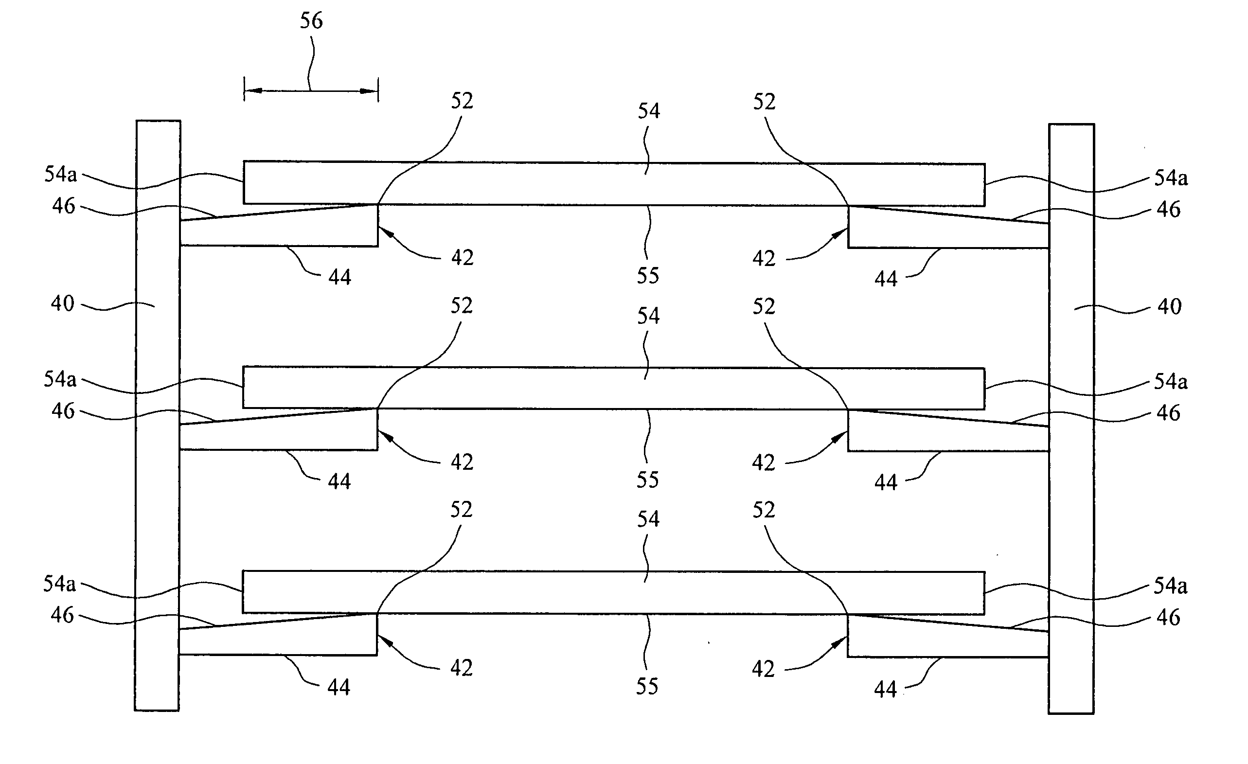
[0026] The present invention contemplates a wafer boat which is suitable for holding multiple wafers in a vertical processing furnace and eliminating or at least substantially reducing wafer warpage and particle generation during processing of the wafers. In an illustrative embodiment, the wafer boat includes a base plate and multiple vertical support rods extending from the base plate. Multiple wafer support pins extend from each support rod in vertically-spaced relationship to each other. A wafer support pin on each support rod, in conjunction with a wafer support pin on each of the other support rods, supports a corresponding one of the wafers during processing. Each wafer support pin has a generally tapered configuration such that the upper surface of each wafer support pin is disposed at an acute angle with respect to the longitudinal axis of the support rod. When a wafer is supported on the wafer support pins, the contact surface area of each wafer support pin with the backsid...


PUM

PropertyMeasurementUnit
acute angleaaaaaaaaaa
lengthaaaaaaaaaa

Abstract

A wafer boat which is suitable for supporting wafers in a process furnace is disclosed. The wafer boat includes a base plate, multiple support rods carried by the base plate and multiple wafer support pins carried by each of the support rods. Each of the wafer support pins has an upper surface disposed at an acute angle with respect to a longitudinal axis of each of the support rods. This causes contact of the wafer support pins with the wafer at the wafer's center of gravity and minimizes the contact surface area between the wafer support pins and each wafer.

Description

FIELD OF THE INVENTION [0001] The present invention relates to furnaces used in the fabrication of semiconductor integrated circuits on semiconductor wafer substrates. More particularly, the present invention relates to a wafer boat having angled wafer support pins which contact a wafer at the center of gravity of the wafer to prevent or reduce wafer warpage and particle generation during processing. BACKGROUND OF THE INVENTION [0002] The fabrication of various solid state devices requires the use of planar substrates, or semiconductor wafers, on which integrated circuits are fabricated. The final number, or yield, of functional integrated circuits on a wafer at the end of the IC fabrication process is of utmost importance to semiconductor manufacturers, and increasing the yield of circuits on the wafer is the main goal of semiconductor fabrication. After packaging, the circuits on the wafers are tested, wherein non-functional dies are marked using an inking process and the function...

Claims


Application Information

Patent Timeline
Patent Type & Authority Applications(United States)
IPC IPC(8): C23C16/00
CPCH01L21/67309C23C16/4583
Inventor HSU, CHUN-KENGLIN, CHUN-CHIH
Owner TAIWAN SEMICON MFG CO LTD
Why Eureka
Try Eureka