Cleaning submicron structures on a semiconductor wafer surface

a technology of semiconductor wafers and submicron structures, applied in the field of semiconductor processing, can solve the problems of affecting the performance of the substrate, so as to achieve the effect of reducing surface tension and expending heat energy

Inactive Publication Date: 2006-03-02
APPLIED MATERIALS INC
View PDF20 Cites 92 Cited by
  • Summary
  • Abstract
  • Description
  • Claims
  • Application Information

AI Technical Summary

Problems solved by technology

These structures are fragile due to their increasingly small dimensions and the types of materials used to form the structures.
Polysilicon is a fragile material, particularly when it is part of a gate stack formed on a thin silicon oxide layer.
The use of acoustic energy was found to cause significant damage in combination with aqueous solutions.
But, using only an aqueous solution does not adequately clean the surfaces of submicron structures having a dimension of 0.15 μm or less and therefore may cause the loss of critical dimension control and ultimately cause lower yields.
Also, because the amine based cleaning solution was developed for removing mainly organic residues, it is not as effective at cleaning mostly inorganic residues.
Additionally, the amines left over after cleaning may cause photoresist poisoning in later steps.
Additionally, the solvents and the chemical additives used in amine-based cleaning solutions are expensive and difficult to dispose of in an environmentally friendly manner.
Additionally, the aqueous HF cleaning solution and the aqueous oxalic acid cleaning solution do not remove residues to the extent necessary to provide the desired critical dimension control and improved yield.
Cleaning both sides of the wafer using the dual spray method has the drawback of the splashing 145 caused by spraying a cleaning solution onto the bottom of a wafer.
The splashing will result in the mixing of the cleaning solution applied to the top 130 and the bottom 135 of the wafer 140, therefore making it difficult to use two different cleaning solutions on the top and the bottom of the wafer, particularly where the mixing of the two cleaning solutions would result in the degradation of one or both of the cleaning solutions.

Method used


Image

  • Cleaning submicron structures on a semiconductor wafer surface
  • Cleaning submicron structures on a semiconductor wafer surface
  • Cleaning submicron structures on a semiconductor wafer surface

Examples


Embodiment Construction

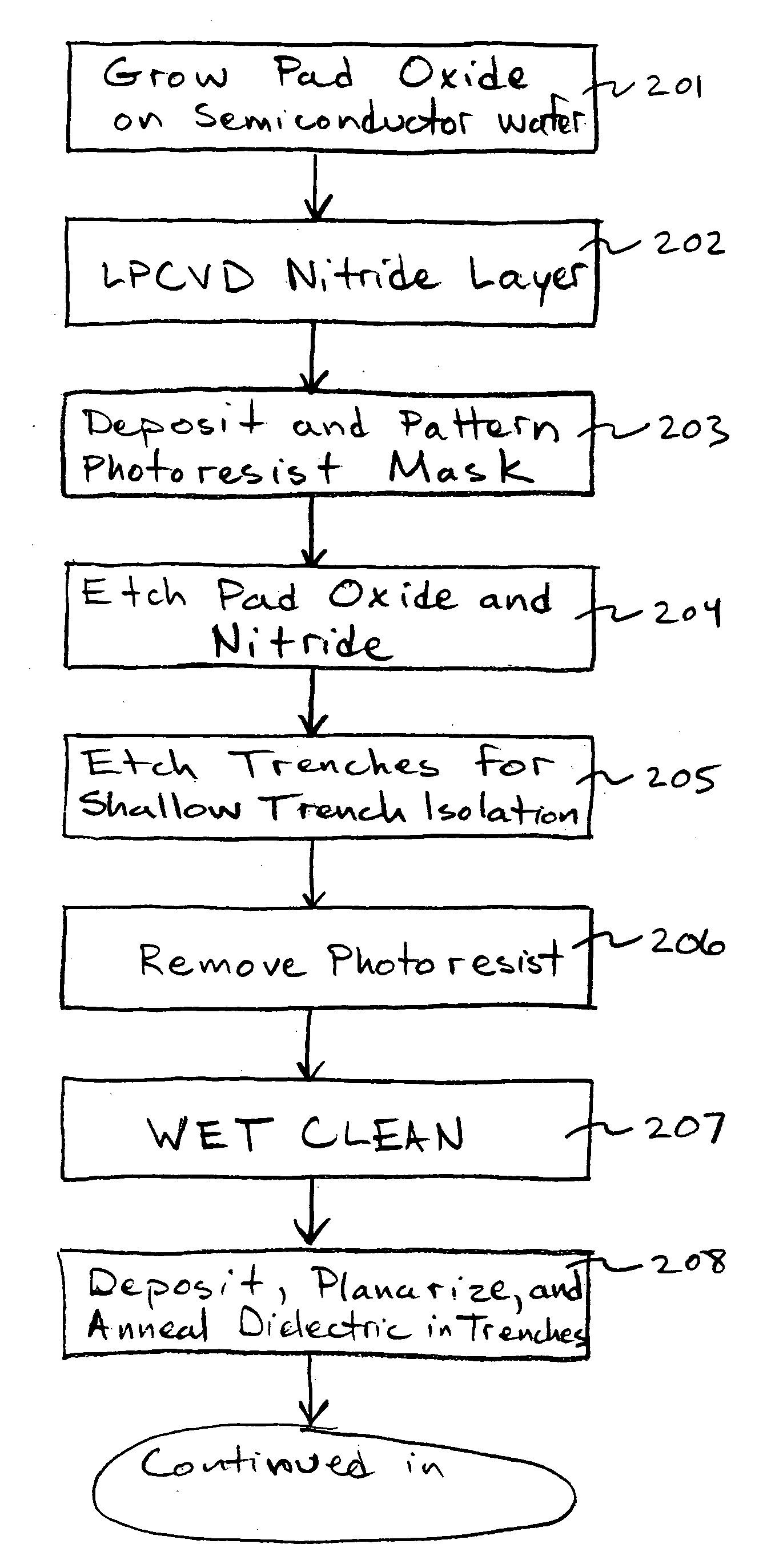
[0023] In the following description numerous specific details are set forth in order to provide a thorough understanding of the present invention. One of ordinary skill in the art will understand that these specific details are for illustrative purposes only and are not intended to limit the scope of the present invention. Additionally, in other instances, well-known processing techniques and equipment have not been set forth in particular detail in order to not unnecessarily obscure the present invention.

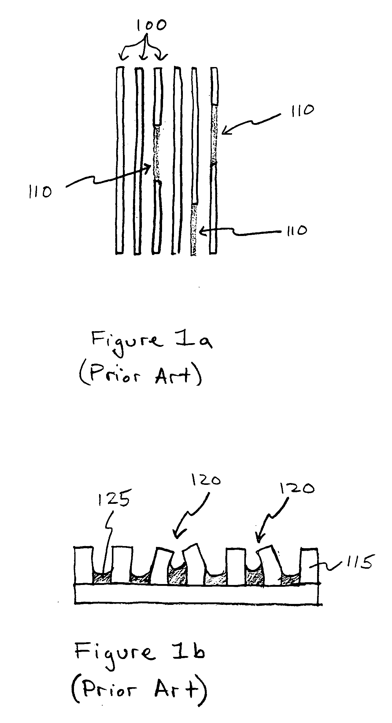
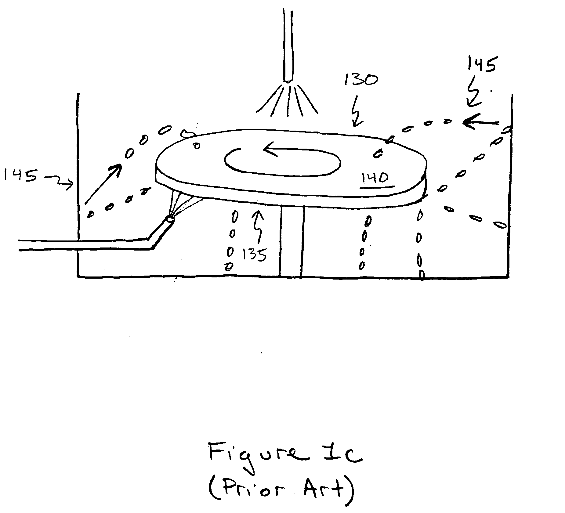
[0024] Fragile structures having a dimension below 0.15 μm and fragile materials such as polysilicon may be cleaned with a cleaning solution in combination with acoustic energy without harming the structures by formulating a cleaning solution from a solvent having a surface tension lower than that of water. This cleaning solution formulated from a solvent having a surface tension lower than that of water may be used to clean structures formed during front-end-of-the-line (FEOL) pr...


PUM

PropertyMeasurementUnit
frequencyaaaaaaaaaa
depthaaaaaaaaaa
thicknessaaaaaaaaaa

Abstract

Cleaning solutions and cleaning methods targeted to particular substrates and structures in semiconductor fabrication are described. A method of cleaning fragile structures having a dimension less than 0.15 um with a cleaning solution formed of a solvent having a surface tension less than water while applying acoustic energy to the substrate on which the structures are formed is described. Also, a method of cleaning copper with several different cleaning solutions, and in particular an aqueous sulfuric acid and HF cleaning solution, is described. Also, methods of cleaning both sides of a substrate at the same time with different cleaning solutions applied to the top and the bottom are described.

Description

BACKGROUND OF THE INVENTION [0001] 1. Field of the Invention [0002] The present invention relates to the field of semiconductor processing and more particularly to cleaning a semiconductor substrate with cleaning solutions tailored to clean particular surfaces on the semiconductor substrate during processing. [0003] 2. Discussion of Related Art [0004] The surfaces of semiconductor substrates may be cleaned at several points during the fabrication of structures on the semiconductor substrates. The cleaning requirements vary for different materials and different structures. The cleaning requirements for surfaces before metallization (front-end-of-the-line) may be different from the cleaning requirements after metallization (back-end-of-the-line). In the past, front-end-of-the-line (FEOL) cleaning was performed using aqueous solutions. In the FEOL, shallow trench isolation structures and gate or memory stacks are typically formed. These structures are fragile due to their increasingly ...

Claims


Application Information

Patent Timeline
Patent Type & Authority Applications(United States)
IPC IPC(8): B08B3/12
CPCB08B3/08B08B3/12C11D7/08C11D11/0047C11D11/007H01L21/76814H01L21/02071H01L21/02074H01L21/0209H01L21/67051H01L21/76808H01L21/02063
Inventor VERHAVERBEKE, STEVENTANG, JIANSHEGOUK, ROMANBROWN, BRIAN J.CHEN, HAN-WENWENG, CHING-HWAPAPANU, JAMES S.YOST, DENNIS
Owner APPLIED MATERIALS INC
Why Eureka
Try Eureka