

Imaging device and imaging system
a technology of imaging device and imaging system, which is applied in the direction of television system scanning details, radioation control devices, television systems, etc., can solve the problem of difficult to secure a sufficient area for the photodiod
- Summary
- Abstract
- Description
- Claims
- Application Information
AI Technical Summary
Benefits of technology
Problems solved by technology
Method used
Image

Examples
embodiment 1
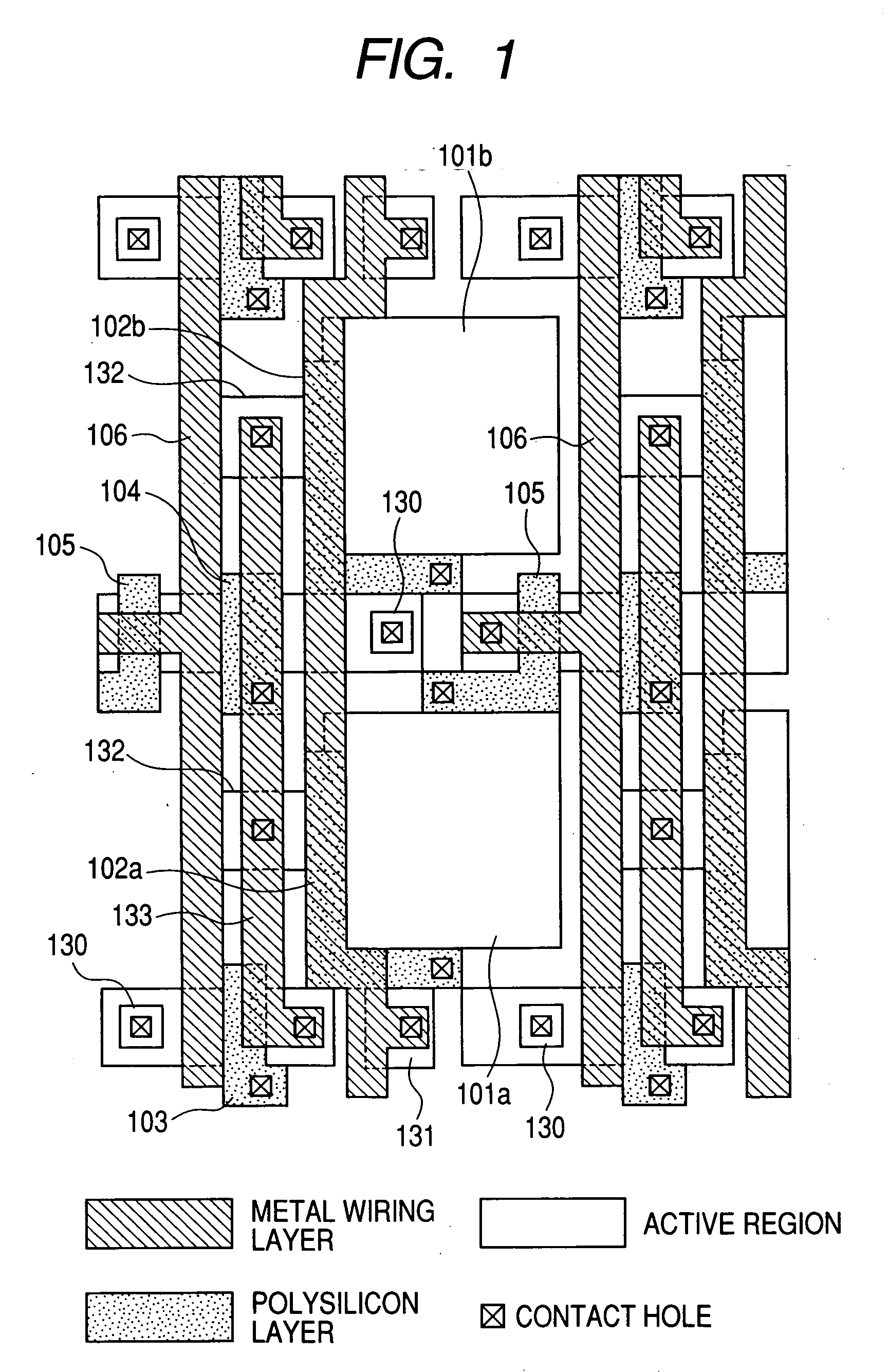
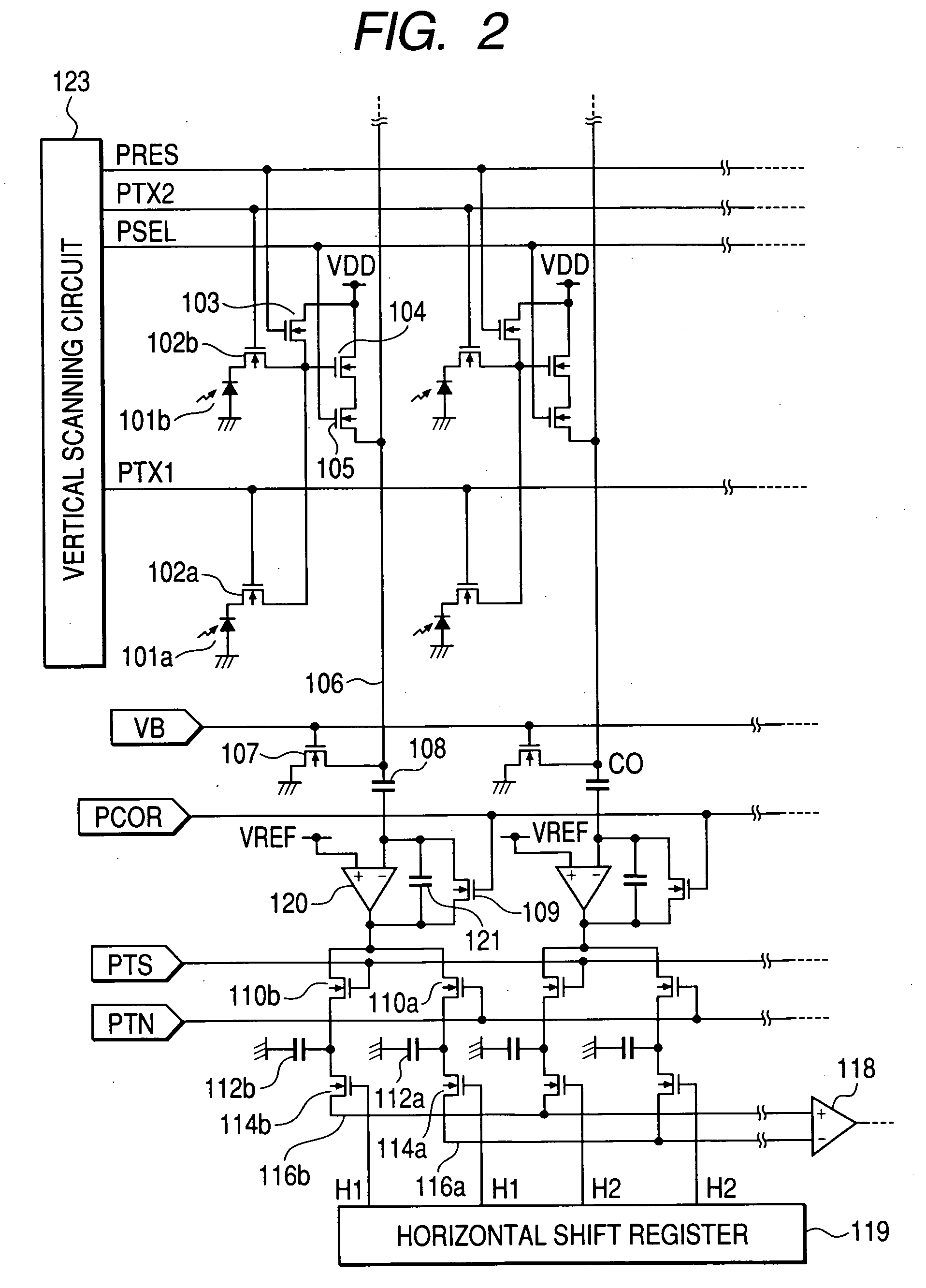
[0031] An imaging device according to a first embodiment of the present invention will be described. FIG. 1 is a plan view of a unit cell of an imaging device according to the first embodiment. FIG. 2 is an equivalent circuit diagram of the imaging device according to the present embodiment, in which pixels having the layout shown in FIG. 1 are disposed two-dimensionally.
[0032] In FIG. 2, the unit cell includes photodiodes 101A and 101B being a photoelectric conversion element, and a common amplification MOSFET 104 which amplifies signals generated in the photodiodes 101A and 101B, and further, a reset MOSFET 103 acting as a common reset switch which resets the input of the amplification MOSFET 104 to a predetermined voltage, and a row selecting MOSFET 105 acting as a common row selecting switch which controls conduction between the source electrode of the amplification MOSFET 104 and a vertical output line 106. In addition, transfer MOSFET 102A and MOSFET 102B acting as a transfer...
embodiment 2
[0041] An imaging device according to a second embodiment of the present invention will be described. FIG. 5 is an equivalent circuit diagram of an imaging device according to the second embodiment, in which one portion relating to 2×4 pixels selected from among pixels arranged two-dimensionally is shown. In the imaging device according to the present embodiment, four pixels, sharing an amplification MOSFET, reset MOSFET and row selecting MOSFET, constitute a unit cell. FIG. 6 is a plan view showing a layout of these pixels. In FIGS. 5 and 6, the same reference numerals are applied to constituent components corresponding to FIGS. 2 and 1, and hence repeated explanation thereof is omitted. The shape of the gate electrode of a transfer MOSFET of FIG. 6 is apparently different from that of the gate electrode of a transfer MOSFET of FIG. 1. However, this is due to simplification; actually the shape of the gate electrode of a transfer MOSFET of FIG. 6 is identical to that of the gate ele...
embodiment 3
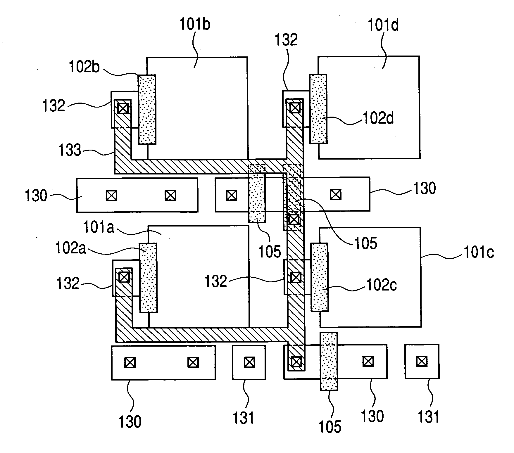
[0044] An imaging device according to a third embodiment of the present invention will be described. The equivalent circuit of an imaging device according to the third embodiment is similar to that of the second embodiment. FIG. 7 is a plan view showing a layout of the pixels. In FIG. 7, the same reference numerals are applied to constituent components corresponding to FIG. 6, and hence repeated explanation thereof is omitted. A reset MOSFET 103, amplification MOSFET 104 and row selecting MOSFET 105 are shared by four pixels, and photodiodes 101A, 101B, 101C and 101D are disposed in lines 4n-3, 4n-2, 4n-1 and 4n, respectively (n being a natural number). A transfer switches 102A, 102B, 102C and 102D are arranged in equivalent positions relative to the photodiodes 101A, 101B, 101C and 101D, respectively, thus having translational symmetry. Consequently, a sensitivity difference between the four pixels does not arise. A feature of the imaging device of the present embodiment is that, a...
PUM
 Abstract
Description
Claims
Application Information