Semiconductor apparatus having stacked semiconductor components

a technology of semiconductor components and semiconductor devices, which is applied in the direction of electrical devices, semiconductor devices, and semiconductor/solid-state device details, etc., can solve the disadvantage of not being able to match the impedance of all wiring sections, the disadvantage of the individual semiconductor components connected to one another's wiring between the contact regions b>10/b>, and the bus system having branches in the signal line, etc., to achieve the effect of improving the wiring

Inactive Publication Date: 2006-03-02
POLARIS INNOVATIONS
View PDF6 Cites 9 Cited by
  • Summary
  • Abstract
  • Description
  • Claims
  • Application Information

AI Technical Summary

Benefits of technology

[0007] It is an object of the present invention to provide a semiconductor apparatus which makes it possible to stack semiconductor components and, at the same time, to provide improved wiring.

Problems solved by technology

The impedance of the wirings between the contact regions 10 of the individual semiconductor components which are connected to one another is disadvantageously not matched in all four of the known semiconductor apparatuses presented.
Another problem results for bus systems having branches in the signal lines.
In this case, it is not easily possible to match the impedance of all wiring sections without additional capacitances and inductances.
Bus systems therefore always have sections with poor impedance matching.
This results in the problem of the performance of future memory components being restricted by signal reflections and interference effects on account of the wiring.

Method used


Image

  • Semiconductor apparatus having stacked semiconductor components
  • Semiconductor apparatus having stacked semiconductor components
  • Semiconductor apparatus having stacked semiconductor components

Examples


second embodiment

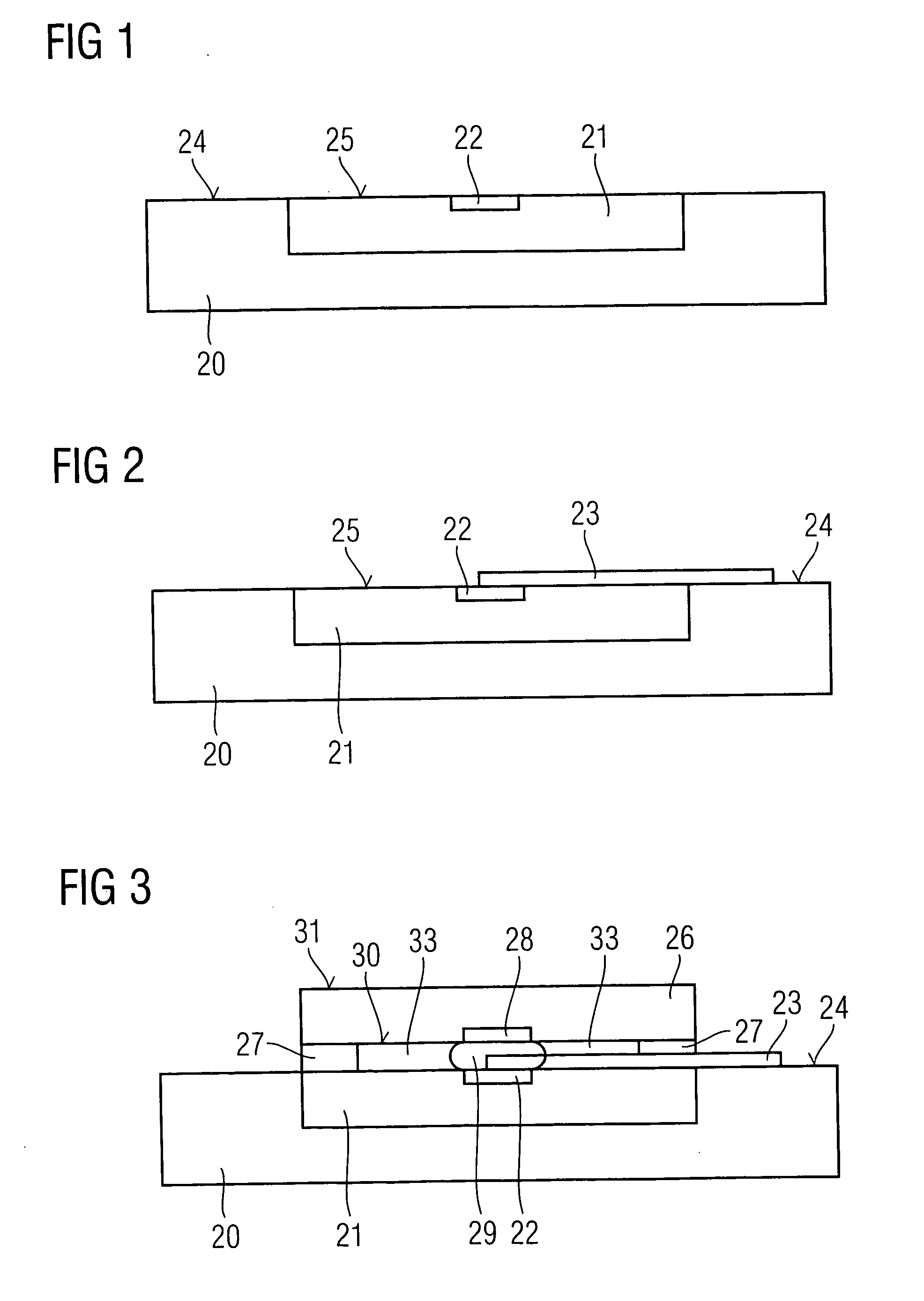
[0025] A diagrammatic illustration of the present invention is described in FIG. 7. After a first semiconductor component 21 has been embedded in the potting compound 20 and a rewiring 23 has been formed, a dielectric layer 40 is deposited. The dielectric layer 40 is configured in such a manner that it does not cover an external region of the rewiring 23 in the region of the potting compound 20. A conductive layer 41 is deposited onto the dielectric layer. This conductive layer 41 then forms an equipotential surface or an earth surface. In the case of a given electric constant of the dielectric 40 and the typical frequencies of the semiconductor component, the thickness of the dielectric layer 40 and the width of the wiring 23 are selected, in accordance with known techniques or knowledge of electrodynamics, in such a manner that it is possible to match the impedance in an optimum manner.

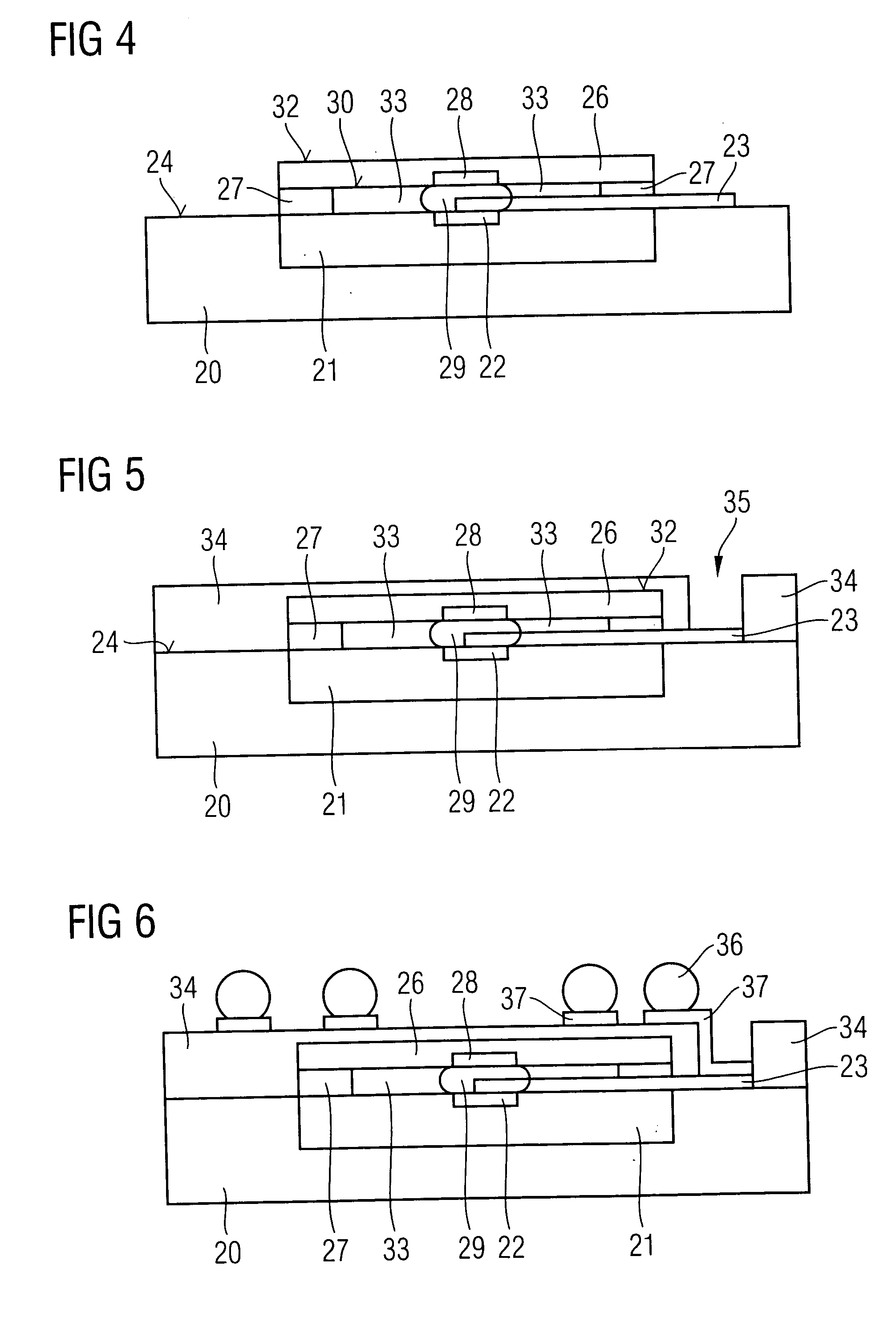
[0026] In subsequent steps, as described in the first exemplary embodiment, a second semiconduct...

third embodiment

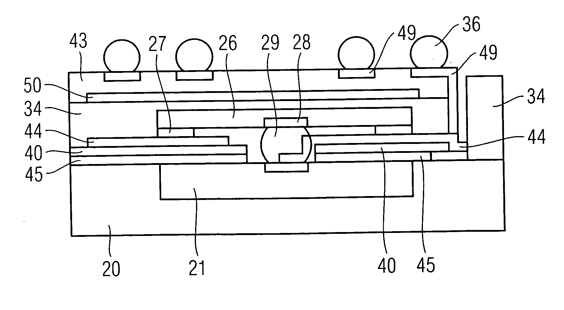
[0027]FIGS. 9 and 10 illustrate a third embodiment of the present invention. This embodiment differs from the second embodiment by virtue of the fact that an equipotential or earth surface 45 is applied to the first embedded semiconductor component 21 in a first step. This earth surface 45 does not touch the contact-connection region 22. A dielectric layer 40 is deposited onto the earth surface 45. A rewiring 44 is then formed. This rewiring contact-connects the contact-connection region 22. The impedance of this rewiring is matched using the earth surface 45 and the dielectric layer 40. The subsequent steps for producing the present invention correspond to those of the second embodiment.

[0028] Although the present invention was described with reference to preferred exemplary embodiments, it is not restricted thereto. In particular, various techniques are known in order to fasten the second semiconductor component on the first semiconductor component. Furthermore, the materials for ...


PUM


Abstract

The present invention provides an apparatus having stacked semiconductor components. Two semiconductor components (21, 26) are arranged such that their contact regions (28, 22) are opposite one another. A contact-connection device (29) forms a short electrical connection between the two contact regions (28, 22). The contact regions (28, 22) are connected to external contact regions (36) of the apparatus via a rewiring (23).

Description

TECHNICAL FIELD [0001] The present invention relates to a semiconductor apparatus having stacked semiconductor components. The present invention also relates to a method for producing the semiconductor apparatus according to the invention. BACKGROUND ART [0002] Although the present invention is described with reference to memory components, the invention is not restricted thereto. [0003] Memory components are connected to one another via a bus system, for example. The wiring paths provided, in particular of the signal lines, should be as short as possible. One technique provides for stacking memory components. The length of the wirings between contacts which are located above one another is kept short in this manner. FIG. 11 illustrates one known arrangement of housed semiconductor components 5. Two housed semiconductor components are placed on top of one another and are electrically connected to one another via the external wiring 3. FIG. 12 illustrates another arrangement for stac...

Claims


Application Information

Patent Timeline
Patent Type & Authority Applications(United States)
IPC IPC(8): H01L21/50H01L23/02
CPCH01L25/0657H01L2224/32145H01L2924/15311H01L2224/32245H01L2224/32225H01L2924/3011H01L2924/30107H01L2924/01078H01L2225/06586H01L2225/06527H01L2225/06524H01L2225/06513H01L2224/73265H01L2224/48465H01L2224/48247H01L2224/48227H01L2924/00H01L2924/00012H01L24/73H01L2924/181
Inventor HEDLER, HARRYIRSIGLER, ROLANDMEYER, THORSTEN
Owner POLARIS INNOVATIONS
Why Eureka
Try Eureka