Carrier structure for stacked-type semiconductor device, method of producing the same, and method of fabricating stacked-type semiconductor device

a semiconductor device and carrier structure technology, applied in semiconductor devices, semiconductor/solid-state device details, electrical devices, etc., can solve the problems of reducing production yield, difficult to obtain even plate thickness, and high production cost, and achieve the effect of improving production yield

Inactive Publication Date: 2006-03-02
MONTEREY RES LLC
View PDF3 Cites 17 Cited by
  • Summary
  • Abstract
  • Description
  • Claims
  • Application Information

AI Technical Summary

Benefits of technology

[0012] The present invention has been made taking the above into consideration, and has an object of providing a carrier structure for stacked-type semiconduct...

Problems solved by technology

In case where the lower carrier is formed by scraping of metal, there is a difficulty in obtaining the even plate thickness and the carrier is likely to be warped.
If this lower carrier is used for the fabrication of the stacked-type semiconductor devices, the lower carrier may cause a mis...

Method used


Image

  • Carrier structure for stacked-type semiconductor device, method of producing the same, and method of fabricating stacked-type semiconductor device
  • Carrier structure for stacked-type semiconductor device, method of producing the same, and method of fabricating stacked-type semiconductor device
  • Carrier structure for stacked-type semiconductor device, method of producing the same, and method of fabricating stacked-type semiconductor device

Examples


Embodiment Construction

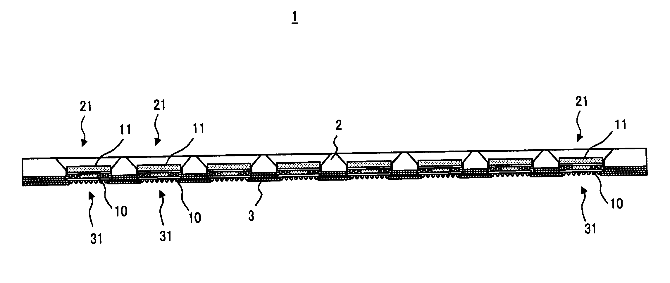
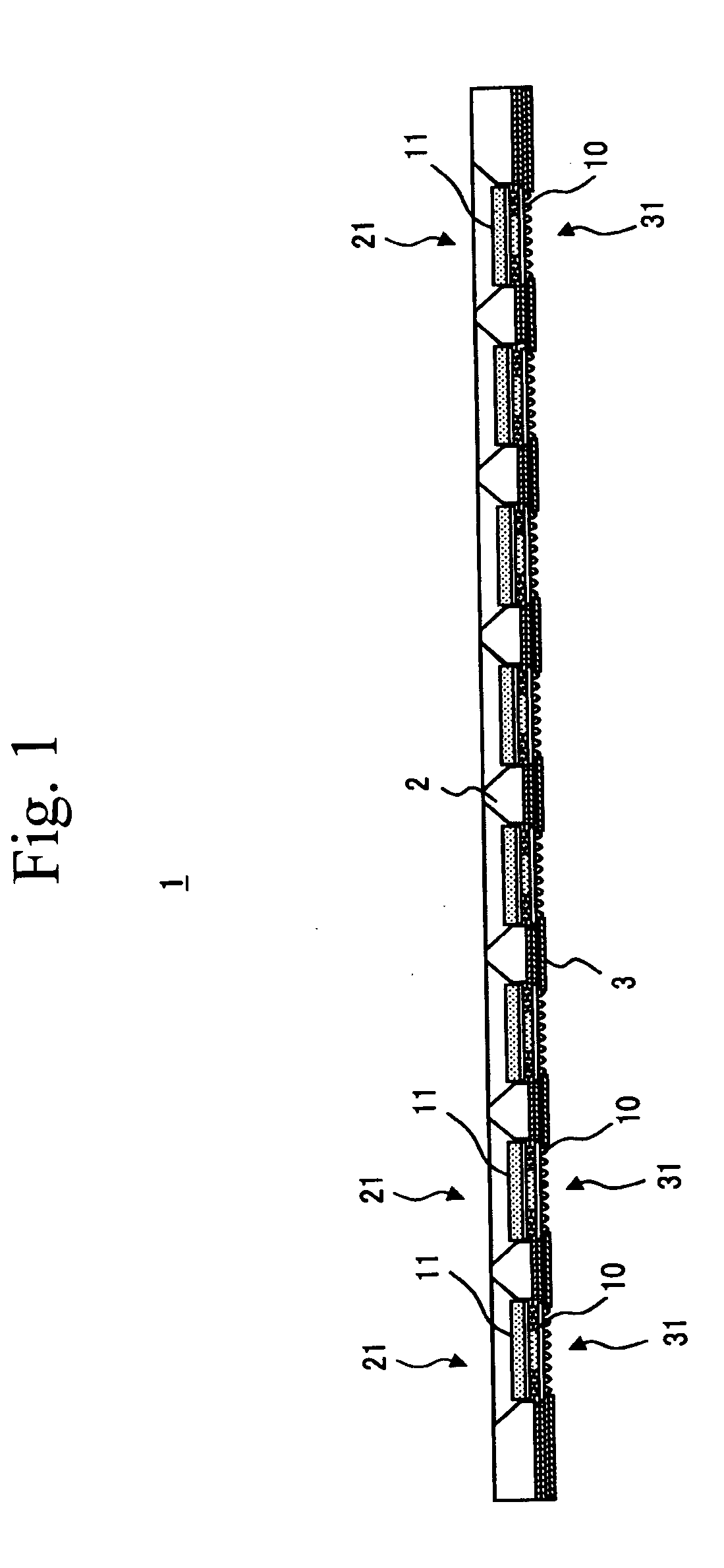
[0035] A description will now be given of preferred embodiments of the present invention with reference to the accompanying drawings. FIG. 1 is a cross-sectional view of a carrier structure for fabricating a stacked-type semiconductor device according to an embodiment of the present invention (hereinafter, the carrier structure may be simply referred to as carrier). Referring to FIG. 1, a carrier 1 is composed of an upper carrier 2 and a lower carrier 3. The lower carrier 3 has a plurality of openings 31 for mounting first semiconductor packages 10, and is composed of multiple thin plates stacked. Each thin plate may be stainless. The upper carrier 2 has a plurality of openings 21 for mounting semiconductor packages 11 on the first semiconductor packages 10. The upper carrier 2 may be made of aluminum. The upper carrier 2 is stacked on the lower carrier 3, and the first semiconductor packages 10 are mounted so as to cover the openings 31. Then, the second semiconductor packages 11 a...


PUM


Abstract

A carrier structure for fabricating a stacked-type semiconductor device includes: a lower carrier that has laminated thin plates and has first openings for mounting first semiconductor packages thereon; and an upper carrier having second openings for mounting second semiconductor packages on the first semiconductor packages. The lower carrier composed of the laminated thin plates realizes an even plate thickness and reduces warps because stress is distributed to the thin plates. This results in an improved production yield. A pattern of the openings in the thin plates of the lower carrier may be formed by etching or electric discharging. The openings thus formed have reduced warps and burrs.

Description

CROSS REFERENCE TO RELATED APPLICATIONS [0001] This is a continuation of International Application No. PCT / JP2004 / 012476, filed Aug. 30, 2004. BACKGROUND OF THE INVENTION [0002] 1. Field of the Invention [0003] The present invention relates to a carrier structure for stacked-type semiconductor devices, a method of producing the carrier structure, and a method of fabricating a stacked-type semiconductor device, and more particularly, to a carrier structure for a stacked-type semiconductor device having semiconductor packages stacked and packaged into a single semiconductor package, a method of producing this type of carrier structure, and a method of fabricating the stacked-type semiconductor device. [0004] 2. Description of the Related Art [0005] Recently, portable electronic equipment such as a movable phone, and non-volatile recording media such as IC memory cards have been downsized, and it has been required to reduce the number of components used in the apparatuses and recording...

Claims


Application Information

Patent Timeline
IPC IPC(8): H01L23/48
CPCH01L21/67336H01L2924/3511H01L25/50H01L21/6835H01L25/105H01L2225/1023H01L25/0657H01L2225/06513H01L2224/32145H01L2225/1058
Inventor ONODERA, MASANORIMEGURO, KOUICHIKASAI, JUNICHISHINMA, YASUHIROTAYA, KOJITANAKA, JUNJI
Owner MONTEREY RES LLC
Why Eureka
Try Eureka