Organic thin film, method of producing the same, and field effect transistor using the same
a technology of field effect transistor and organic thin film, which is applied in the direction of thermoelectric devices, instruments, optics, etc., can solve the problems of small alignment control force of grating, need cleaning steps, static electricity and damage of aligned films, etc., and achieve high smoothness
- Summary
- Abstract
- Description
- Claims
- Application Information
AI Technical Summary
Benefits of technology
Problems solved by technology
Method used
Image

Examples
example 1
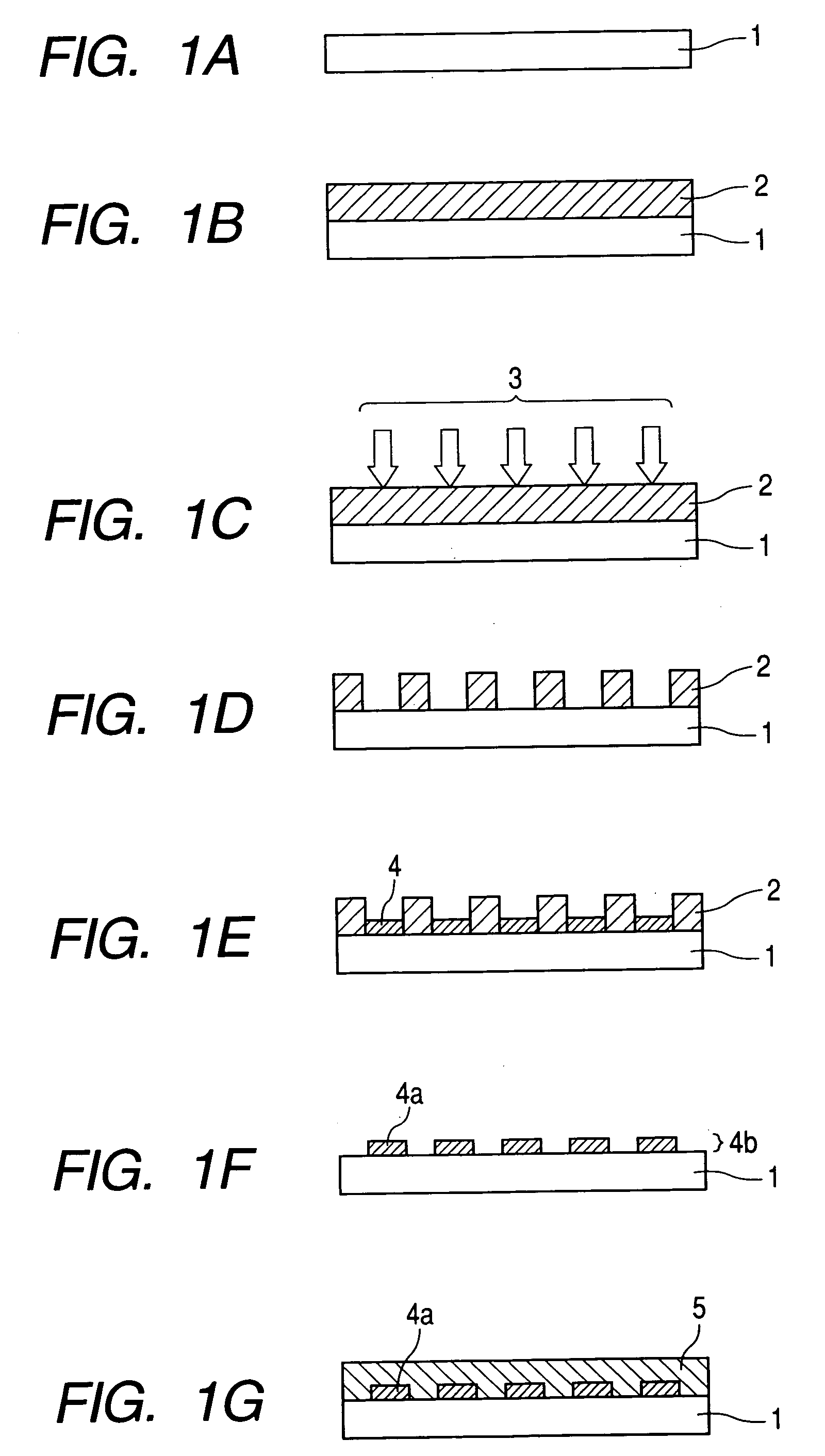
[0055]FIGS. 1A to 1G collectively show a production process for an organic thin film of Example 1.
[0056] An electron beam resist 2 was formed on a glass substrate 1 by spin coating. Next, the electron beam resist 2 was irradiated with an electron beam 3, to thereby form a resist pattern with a width of 370 nm and a pitch of 650 nm.
[0057] Then, the glass substrate 1 having formed thereon the electron beam resist 2 with a pitch of 650 nm was immersed in a hexadecane solution (0.06 mol / l) of octadecyltrichlorosilane for 1 hour, and was taken out. The glass substrate 1 taken out was subjected to ultrasonic cleaning in hexadecane for 2 minutes, and then subjected to ultrasonic cleaning twice in chloroform for 2 minutes each. In this way, the electron beam resist 2 was peeled off, and a pattern of octadecyltrichlorosilane as an insulating region 4a with a different surface energy density from that of the glass substrate 1 was formed on the glass substrate 1. The surface treated region 4...
example 2
[0061]FIGS. 1A to 1G collectively show a production process for an organic thin film of Example 2.
[0062] An electron beam resist 2 was formed on a glass substrate 1 by spin coating. Next, the electron beam resist 2 was irradiated with an electron beam 3, to thereby form a resist pattern with a pitch of 80 nm.
[0063] Then, the glass substrate 1 having formed thereon the electron beam resist 2 with a pitch of 80 nm was immersed in a hexadecane solution (0.06 mol / l) of tridecafluoro-tetrahydrooctyl-trichlorosilane for 1 hour, and was taken out. The glass substrate 1 taken out was subjected to ultrasonic cleaning in hexadecane for 2 minutes, subjected to ultrasonic cleaning twice in chloroform for 2 minutes each, and subjected to ultrasonic cleaning twice in perfluoroacetic acid for 5 minutes each. In this way, the electron beam resist 2 was peeled off, and a pattern of tridecafluoro-tetrahydrooctyl-trichlorosilane as an insulating region 4a with a different surface energy density from...
example 3
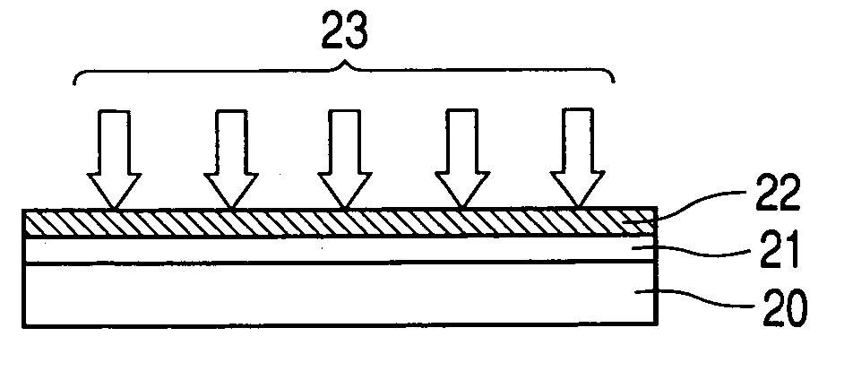
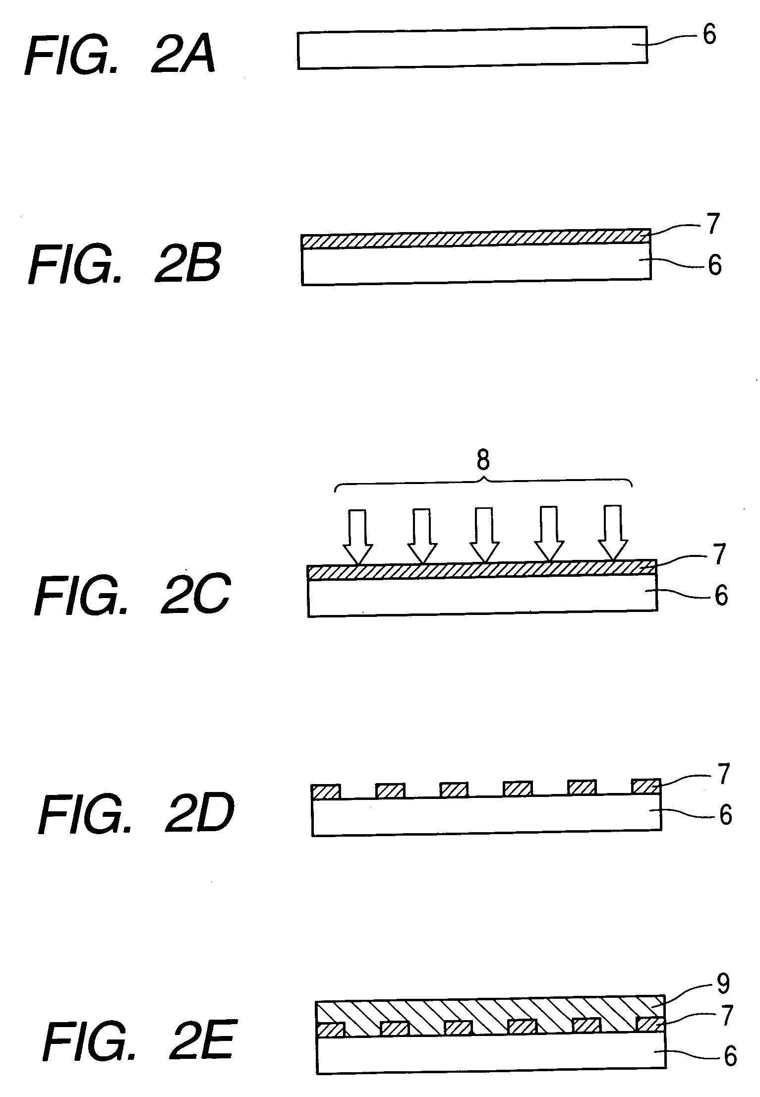
[0067]FIGS. 2A to 2E collectively show a production process for an organic thin film of Example 3.
[0068] A silicon substrate 6 was immersed in a chloroform solution (0.06 mol / l) of octadecyltrichlorosilane for 1 hours, and was taken out. The silicon substrate 6 taken out was subjected to ultrasonic cleaning twice in chloroform for 2 minutes each, to thereby form uniformly a coupling agent octadecyltrichlorosilane 7 on the silicon substrate 6.
[0069] Then, octadecyltrichlorosilane 7 formed was irradiated with an electron beam 8, to thereby form a pattern including octadecyltrichlorosilane 7 with a pitch of 650 nm and the surface of the silicon substrate 6 on the silicon substrate 6.
[0070] A surface energy density of the silicon substrate alone was measured, resulting in 74.4 dyne / cm. A surface energy density of the silicon substrate uniformly subjected to octadecyltrichlorosilane treatment was measured, resulting in 23.5 dyne / cm. Thus, a difference in surface energy density between...
PUM
| Property | Measurement | Unit |
|---|---|---|
| surface roughness | aaaaa | aaaaa |
| thickness | aaaaa | aaaaa |
| thickness | aaaaa | aaaaa |
Abstract
Description
Claims
Application Information
 - R&D Engineer
- R&D Manager
- IP Professional
- Industry Leading Data Capabilities
- Powerful AI technology
- Patent DNA Extraction
Browse by: Latest US Patents, China's latest patents, Technical Efficacy Thesaurus, Application Domain, Technology Topic.
© 2024 PatSnap. All rights reserved.Legal|Privacy policy|Modern Slavery Act Transparency Statement|Sitemap