

Mult-interface auto-switch circuit and memory device with dual interface auto-switch circuit
- Summary
- Abstract
- Description
- Claims
- Application Information
AI Technical Summary
Benefits of technology
Problems solved by technology
Method used
Image

Examples
first embodiment
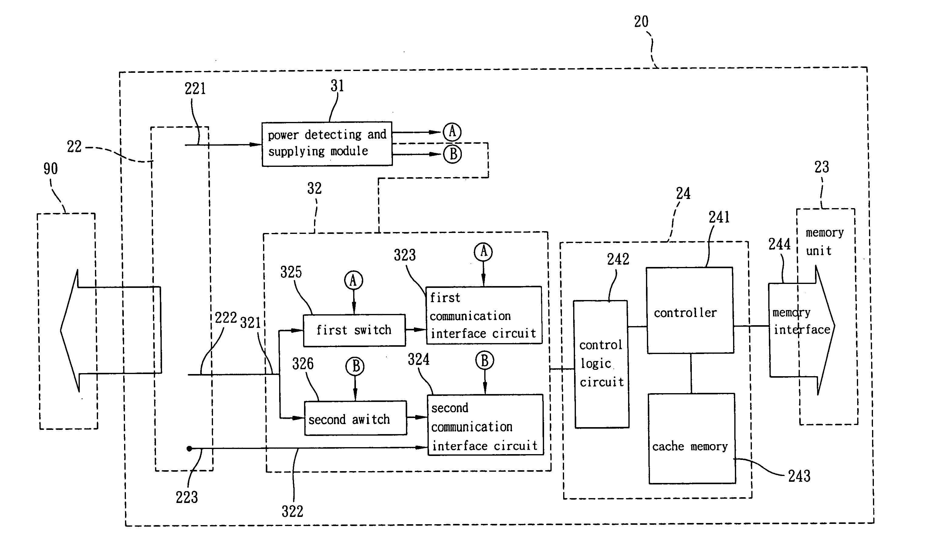
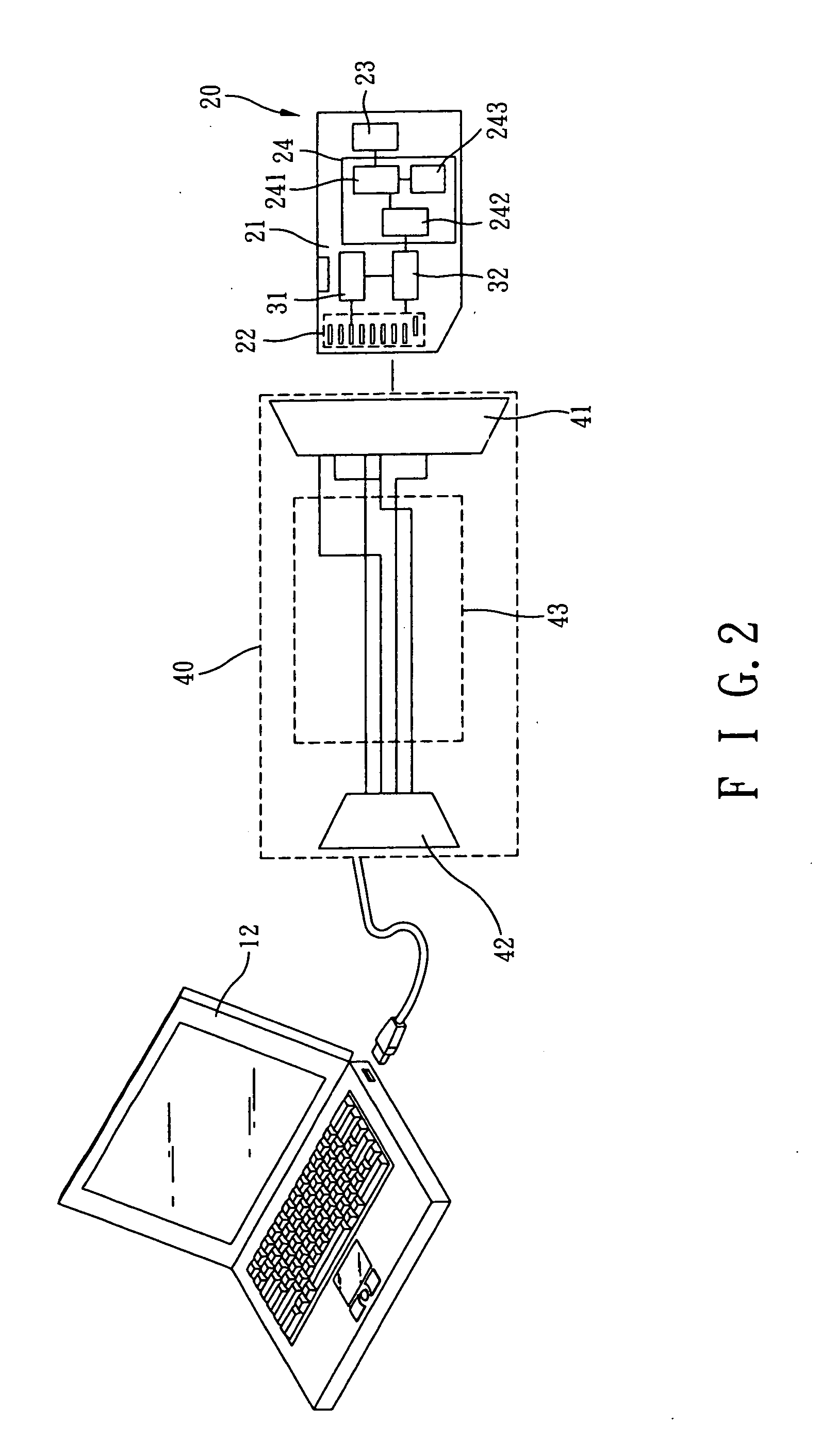
[0023] Please refer to FIG. 2 and FIG. 3. FIG. 2 and FIG. 3 show an embodiment of the dual-interface auto-switch circuit and the memory device 20 which comprises the dual interface auto-switch circuit. FIG. 2 shows a block diagram of an embodiment of the memory device with a dual-interfaces auto-switch circuit according to the present invention and a computer. FIG. 3 shows a detailed block diagram of the dual-interfaces auto-switch circuit according to the present invention.
[0024] As shown in FIG. 2 and FIG. 3, the memory device 20 of this invention comprises a body 21, connection pins 22, a memory unit 23, a control unit 24, and the dual interface auto-switch circuit of this invention. The dual interface auto-switch circuit of this invention comprises a power detecting and supplying module 31 and an interface switch circuit 32.
[0025] The size of the body 21 fits the size of the flash memory card. In this embodiment, the memory device 20 is a Secure Digital Card (SD). The connectio...
second embodiment
[0049]FIG. 7 illustrates a block diagram of a dual-interfaces auto-switch circuit according to the present invention. The memory device 20 in FIG. 7 also comprises a body 21, a plurality of connection pins 22, a memory unit 23, a control unit 24, and the dual interface auto-switch circuit of this invention. The dual interface auto-switch circuit comprises a power detecting and supplying module 31 and interface switch circuit 32. The embodiment in FIG. 7 is different from the previous embodiment due to that the power detecting and supplying module 31 in FIG. 7 also comprises a power detecting circuit 311 and a regulating circuit 312. The power detecting circuit 311 can compare the received voltage with a predetermined value and transform the received voltage into either the first power signal A or the second power signal B according to the result of comparison. Through the regulating circuit 312, the voltage supplied to the interface switch circuit 32 is stable and the first power si...
PUM
 Abstract
Description
Claims
Application Information