Drive device of light emitting display panel

a technology of light-emitting display panels and drive devices, which is applied in static indicating devices, instruments, electroluminescent light sources, etc., can solve the problems of large power loss as a voltage drop, difficult to accurately express intensity gradation to input video signals, and brought about by large power loss, so as to improve the utilization efficiency of electrical power.

Inactive Publication Date: 2006-03-16
TOHOKU PIONEER CORP
View PDF7 Cites 32 Cited by
  • Summary
  • Abstract
  • Description
  • Claims
  • Application Information

AI Technical Summary

Benefits of technology

[0018] The present invention has been developed based on the above-described technical viewpoint, and it is an object of the present invention to provide a drive device of a light emitting display panel in which an appropriate drive voltage can be constantly supplied from the power supply section to a display panel side to further improve the utilization efficiency of electrical power by comprising a control mode by which the progression rate of aging of the monitoring element roughly coincides with the progression rate of aging of self light emitting elements constituting a display panel.

Problems solved by technology

The organic EL element also has a problem that variations in initial intensities occur due to for example variations in deposition at the time of film formation of this element, and thus it becomes difficult to express intensity gradation faithful to an input video signal.
However, a case hardly occurs where the voltage value obtained by adding the maximum values of the respective voltages as described above is needed as the drive voltage Vo supplied to the constant current circuit, and in a usual state, a large power loss as a voltage drop in the constant current circuit is brought about.
Accordingly, even when the drive voltage provided from the power supply section is controlled while the forward voltage obtained from the monitoring element is utilized as in the structure disclosed in Japanese Patent Application Laid-Open No. 2003-162255, it becomes impossible to maintain the utilization efficiency of electrical power in the power supply section at an optimum state.
That is, since the forward voltage obtained from the monitoring element and the average forward voltage of self light emitting elements constituting a display panel have different progression rates of agings, they gradually dissociate, and it becomes impossible to constantly supply an optimum drive voltage from the power supply section in response to the advance of aging of the self light emitting elements constituting the display panel.
Thus, there is a problem that useless power consumption is generated in an initial stage or a standard state.

Method used


Image

  • Drive device of light emitting display panel
  • Drive device of light emitting display panel
  • Drive device of light emitting display panel

Examples


first embodiment

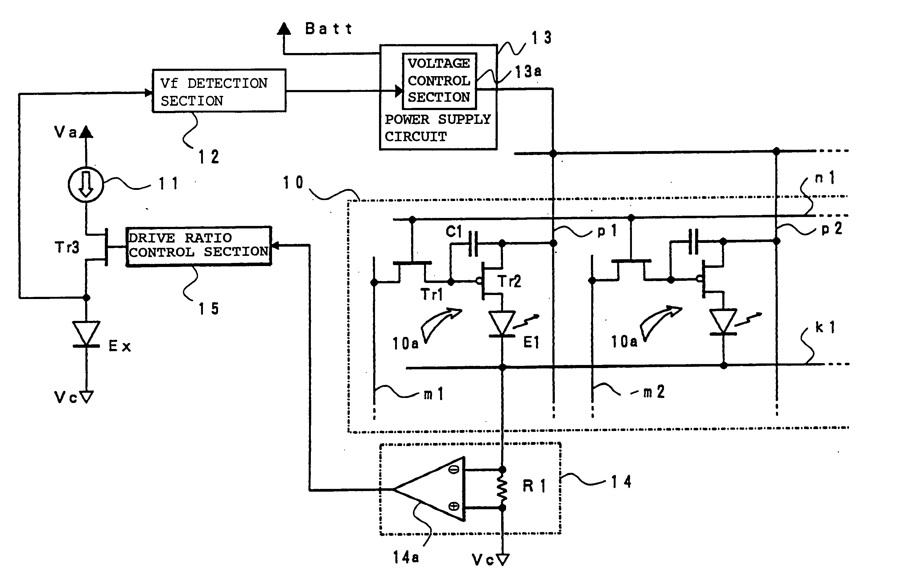
[0027] A drive device of a light emitting display panel according to the present invention will be described below based on embodiments shown in the drawings. FIG. 3 shows a first embodiment thereof and shows the structure of a part of a display panel in which active matrix type display pixels are provided and a block structure of a drive circuit which drives the display panel for lighting it.

[0028] In FIG. 3, in a light emitting display panel designated by reference numeral 10, display pixels 10a are arranged in a matrix pattern. FIG. 3 shows a condition in which only two pixels 10a are arranged in a row direction for convenience of illustration.

[0029] In the light emitting display panel 10, data lines m1, m2, . . . to which a data signal provided from an unillustrated data driver is supplied are arranged in a vertical direction (column direction), and scan selection lines n1, . . . to which a scan selection signal provided from an unillustrated scan driver is supplied are arrange...

second embodiment

[0056]FIG. 6 shows a drive device of a light emitting display panel according to the present invention and shows the structure of a part of the display panel equipped with active matrix type display pixels similarly and a block structure of a drive circuit which drives this part for light emission. In FIG. 6, parts which carry out the same functions as those of the respective parts shown in FIG. 3 already described are designated by the same reference numerals. Accordingly, detailed description thereof will be omitted.

[0057] In the embodiment shown in FIG. 6, the cathodes of respective EL elements E1 arranged in a display panel 10 are respectively connected to the cathode side power supply line Vc. Further, in the embodiment shown in FIG. 6, a detection value by the current consumption detection section 14 is obtained in response to a pulse signal added to a switching element in a DC / DC converter constituting a power supply circuit as described later in detail.

[0058] The drive rati...


PUM


Abstract

In a light emitting display panel 10, a large number of light emitting display pixels 10a are arranged in a matrix pattern, and a monitoring element Ex is provided therein which can extract a voltage which corresponds to the forward voltage of EL elements E1 on the display panel. By a signal from a current consumption detection section 14 which detects current consumption in the light emitting display panel 10, a drive ratio control section 15 performs ON / OFF control of a transistor Tr3 which is connected in series to the monitoring element Ex to control current provided from a constant current circuit. Thus, progression rates of agings of the monitoring element Ex and the EL elements E1 arranged in the display panel can be controlled to roughly coincide with each other, and a power loss generated in a light emission drive transistor Tr2 in each pixel 10a can be restrained as much as possible.

Description

BACKGROUND OF THE INVENTION [0001] 1. Field of the Invention [0002] The present invention relates to a drive device of a light emitting display panel in which a large number of self light emitting elements are arranged in a matrix pattern as display pixels, and more particularly to a drive device of a light emitting display panel in which the display pixels can be driven to be lit efficiently by improvement in the utilization efficiency of electrical power in a power supply section. [0003] 2. Description of the Related Art [0004] Demand for a display panel which has a high definition image display function and which can realize a thin shape and low power consumption has increased due to popularity of cellular telephones, personal digital assistants (PDAS), and the like, and conventionally a liquid crystal display panel has been adopted in many products as the one which meets the needs thereof. Meanwhile, these days a display panel utilizing an organic EL element whose characteristic...

Claims


Application Information

Patent Timeline
Patent Type & Authority Applications(United States)
IPC IPC(8): G09G3/14H05B44/00
CPCG09G3/3233G09G2300/0842G09G2330/021G09G2320/041G09G2320/043G09G2320/029
Inventor YOSHIDA, TAKAYOSHI
Owner TOHOKU PIONEER CORP
Why Eureka
Try Eureka